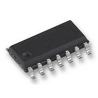
74ABT125D NXP Semiconductors, 74ABT125D Datasheet - Page 3

74ABT125D
Manufacturer Part Number
74ABT125D
Description
Buffer/Line Driver 4-CH Non-Inverting 3-ST BiCMOS 14-Pin SO Tube
Manufacturer
NXP Semiconductors
Specifications of 74ABT125D
Package
14SO
Logic Family
ABT
Logic Function
Buffer/Line Driver
Number Of Outputs Per Chip
4
Output Type
3-State
Input Signal Type
Single-Ended
Maximum Propagation Delay Time @ Maximum Cl
4.6@5V ns
Polarity
Non-Inverting
Supply Voltage Range
4.5V To 5.5V
Logic Case Style
SOIC
No. Of Pins
14
Operating Temperature Range
-40°C To +85°C
Svhc
No SVHC (18-Jun-2010)
Base Number
74
Ic Generic
RoHS Compliant
Package / Case
SOIC
Logic Device Type
Buffer, Non Inverting
Rohs Compliant
Yes
No. Of Circuits
4
Lead Free Status / RoHS Status
Available stocks
Company
Part Number
Manufacturer
Quantity
Price
Part Number:
74ABT125D
Manufacturer:
NXP/恩智浦
Quantity:
20 000
NXP Semiconductors
Table 2.
6. Functional description
Table 3.
[1]
7. Limiting values
Table 4.
In accordance with the Absolute Maximum Rating System (IEC 60134).
[1]
[2]
[3]
74ABT125
Product data sheet
Symbol
1OE to 4OE
1A to 4A
1Y to 4Y
GND
V
Inputs
nOE
L
L
H
Symbol
V
V
V
I
I
I
T
T
P
IK
OK
O
j
stg
CC
CC
I
O
tot
H = HIGH voltage level; L = LOW voltage level; X = don’t care; Z = high-impedance OFF-state.
The input and output voltage ratings may be exceeded if the input and output current ratings are observed.
The performance capability of a high-performance integrated circuit in conjunction with its thermal environment can create junction
temperatures which are detrimental to reliability.
SO14 packages: above 70 C P
SSOP14 and TSSOP20 packages: above 60 C P
DHVQFN14 packages: above 60 C P
Pin description
Function selection
Limiting values
Parameter
supply voltage
input voltage
output voltage
input clamping current
output clamping current
output current
junction temperature
storage temperature
total power dissipation
5.2 Pin description
Pin
1, 4, 10, 13
2, 5, 9, 12
3, 6, 8, 11
7
14
[1]
[1]
tot
derate linearly with 8 mW/K
tot
derate linearly with 4.5 mW/K
nA
L
H
X
All information provided in this document is subject to legal disclaimers.
V
output in LOW-state
T
Conditions
output in OFF-state or HIGH-state
V
Rev. 5 — 24 November 2010
tot
amb
I
O
< 0 V
derate linearly with 5.5 mW/K
< 0 V
= 40 C to +85 C
Description
output enable input (active LOW)
data input
data output
ground (0 V)
supply voltage
Output
nY
L
H
Z
[2]
[3]
Min
0.5
1.2
0.5
18
50
-
-
65
-
74ABT125
Quad buffer; 3-state
+7.0
+7.0
-
128
+150
Max
+5.5
-
150
500
© NXP B.V. 2010. All rights reserved.
Unit
V
V
V
mA
mA
mA
C
C
mW
3 of 16


