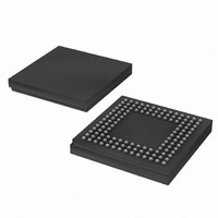
XC2C128-7CPG132I Xilinx Inc, XC2C128-7CPG132I Datasheet - Page 3

XC2C128-7CPG132I
Manufacturer Part Number
XC2C128-7CPG132I
Description
CPLD CoolRunner™-II Family 3K Gates 128 Macro Cells 152MHz 0.18um (CMOS) Technology 1.8V 132-Pin CSBGA
Manufacturer
Xilinx Inc
Series
CoolRunner IIr
Specifications of XC2C128-7CPG132I
Package
132CSBGA
Family Name
CoolRunnerÂ-II
Device System Gates
3000
Number Of Macro Cells
128
Maximum Propagation Delay Time
7.5 ns
Number Of User I/os
100
Number Of Logic Blocks/elements
8
Typical Operating Supply Voltage
1.8 V
Maximum Operating Frequency
152 MHz
Number Of Product Terms Per Macro
40
Operating Temperature
-40 to 85 °C
Programmable Type
In System Programmable
Delay Time Tpd(1) Max
7.0ns
Voltage Supply - Internal
1.7 V ~ 1.9 V
Number Of Logic Elements/blocks
8
Number Of Macrocells
128
Number Of Gates
3000
Number Of I /o
100
Mounting Type
Surface Mount
Package / Case
132-CSBGA
Features
JTAG
Voltage
1.8V
Memory Type
CMOS
Lead Free Status / RoHS Status
Lead free / RoHS Compliant
Number Of Logic Elements/cells
-
Lead Free Status / RoHS Status
Lead free / RoHS Compliant
Available stocks
Company
Part Number
Manufacturer
Quantity
Price
Company:
Part Number:
XC2C128-7CPG132I
Manufacturer:
XILINX
Quantity:
7 483
Part Number:
XC2C128-7CPG132I
Manufacturer:
XILINX/赛灵思
Quantity:
20 000
the same V
CoolRunner-II CPLD I/O standards.)
Table 4: CoolRunner-II CPLD Family Features
Architecture Description
CoolRunner-II CPLD is a highly uniform family of fast, low
power CPLDs. The underlying architecture is a traditional
CPLD architecture combining macrocells into Function
Blocks (FBs) interconnected with a global routing matrix,
the Xilinx Advanced Interconnect Matrix (AIM). The FBs use
a Programmable Logic Array (PLA) configuration which
allows all product terms to be routed and shared among any
of the macrocells of the FB. Design software can efficiently
synthesize and optimize logic that is subsequently fit to the
FBs and connected with the ability to utilize a very high per-
centage of device resources. Design changes are easily
and automatically managed by the software, which exploits
the 100% routability of the Programmable Logic Array within
each FB. This extremely robust building block delivers the
DS090 (v3.1) September 11, 2008
Product Specification
1.
IEEE 1532
I/O banks
Clock division
DualEDGE
Registers
DataGATE
LVTTL
LVCMOS33, 25,
18, and 15
SSTL2_1
SSTL3_1
HSTL_1
Configurable
ground
Quadruple data
security
Open drain outputs
Hot plugging
Schmitt Inputs
LVCMOS15 requires the use of Schmitt-trigger inputs.
(1)
R
CCIO
level. (See
XC2C32A
✓
✓
✓
✓
✓
✓
✓
✓
✓
2
-
-
-
-
-
Table 5
XC2C64A
✓
✓
✓
✓
✓
✓
✓
✓
✓
2
for a summary of
-
-
-
-
-
XC2C128
✓
✓
✓
✓
✓
✓
✓
✓
✓
✓
✓
✓
✓
✓
2
www.xilinx.com
XC2C256
industry’s highest pinout retention, under very broad design
conditions. The architecture is explained in more detail with
the discussion of the underlying FBs, logic and intercon-
nect.
The design software automatically manages these device
resources so that users can express their designs using
completely generic constructs without knowledge of these
architectural details. More advanced users can take advan-
tage of these details to more thoroughly understand the
software’s choices and direct its results.
Figure 1
attach to pins and interconnect to each other within the
internal interconnect matrix. Each FB contains 16 macro-
cells. The BSC path is the JTAG Boundary Scan Control
✓
✓
✓
✓
✓
✓
✓
✓
✓
✓
✓
✓
✓
✓
2
XC2C384
shows the high-level architecture whereby FBs
✓
✓
✓
✓
✓
✓
✓
✓
✓
✓
✓
✓
✓
✓
4
XC2C512
✓
✓
✓
✓
✓
✓
✓
✓
✓
✓
✓
✓
✓
✓
4
CoolRunner-II CPLD Family
3


