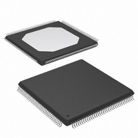
XC2S50E-6TQ144C Xilinx Inc, XC2S50E-6TQ144C Datasheet - Page 9

XC2S50E-6TQ144C
Manufacturer Part Number
XC2S50E-6TQ144C
Description
FPGA Spartan®-IIE Family 50K Gates 1728 Cells 357MHz 0.15um Technology 1.8V 144-Pin TQFP
Manufacturer
Xilinx Inc
Series
Spartan™-IIEr
Datasheet
1.XC2S50E-6TQG144C.pdf
(108 pages)
Specifications of XC2S50E-6TQ144C
Package
144TQFP
Family Name
Spartan®-IIE
Device Logic Cells
1728
Device Logic Units
384
Device System Gates
50000
Maximum Internal Frequency
357 MHz
Typical Operating Supply Voltage
1.8 V
Maximum Number Of User I/os
102
Ram Bits
32768
Number Of Logic Elements/cells
1728
Number Of Labs/clbs
384
Total Ram Bits
32768
Number Of I /o
102
Number Of Gates
50000
Voltage - Supply
1.71 V ~ 1.89 V
Mounting Type
Surface Mount
Operating Temperature
0°C ~ 85°C
Package / Case
144-LQFP
Lead Free Status / RoHS Status
Contains lead / RoHS non-compliant
Other names
122-1204
Available stocks
Company
Part Number
Manufacturer
Quantity
Price
Company:
Part Number:
XC2S50E-6TQ144C
Manufacturer:
XILINX
Quantity:
1 450
Company:
Part Number:
XC2S50E-6TQ144C
Manufacturer:
XILINX
Quantity:
150
Part Number:
XC2S50E-6TQ144C
Manufacturer:
XILINX/赛灵思
Quantity:
20 000
DS077-2 (v2.3) June 18, 2008
Architectural Description
Spartan-IIE FPGA Array
The Spartan
Figure
•
•
•
•
•
© 2003-2007 Xilinx, Inc. All rights reserved. XILINX, the Xilinx logo, the Brand Window, and other designated brands included herein are trademarks of Xilinx, Inc. All other
trademarks are the property of their respective owners.
DS077-2 (v2.3) June 18, 2008
Product Specification
IOBs provide the interface between the package pins
and the internal logic
CLBs provide the functional elements for constructing
most logic
Dedicated block RAM memories of 4096 bits each
Clock DLLs for clock-distribution delay compensation
and clock domain control
Versatile multi-level interconnect structure
3, is composed of five major configurable elements:
®
-IIE user-programmable gate array, shown in
I/O LOGIC
R
DLL
DLL
Figure 3: Basic Spartan-IIE Family FPGA Block Diagram
CLBs
CLBs
www.xilinx.com
0
Spartan-IIE FPGA Family:
Functional Description
Product Specification
As can be seen in
structure with easy access to all support and routing struc-
tures. The IOBs are located around all the logic and mem-
ory elements for easy and quick routing of signals on and off
the chip.
Values stored in static memory cells control all the config-
urable logic elements and interconnect resources. These
values load into the memory cells on power-up, and can
reload if necessary to change the function of the device.
Each of these elements will be discussed in detail in the fol-
lowing sections.
CLBs
CLBs
Figure
DLL
DLL
3, the CLBs form the central logic
DS077_01_052102
9


