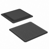
XC3S1600E-5FGG400C Xilinx Inc, XC3S1600E-5FGG400C Datasheet - Page 214

XC3S1600E-5FGG400C
Manufacturer Part Number
XC3S1600E-5FGG400C
Description
FPGA Spartan®-3E Family 1.6M Gates 33192 Cells 657MHz 90nm (CMOS) Technology 1.2V 400-Pin FBGA
Manufacturer
Xilinx Inc
Series
Spartan™-3Er
Datasheet
1.XC3S100E-4VQG100C.pdf
(233 pages)
Specifications of XC3S1600E-5FGG400C
Package
400FBGA
Family Name
Spartan®-3E
Device Logic Cells
33192
Device Logic Units
3688
Device System Gates
1600000
Number Of Registers
29504
Maximum Internal Frequency
657 MHz
Typical Operating Supply Voltage
1.2 V
Maximum Number Of User I/os
304
Ram Bits
663552
Number Of Logic Elements/cells
33192
Number Of Labs/clbs
3688
Total Ram Bits
663552
Number Of I /o
304
Number Of Gates
1600000
Voltage - Supply
1.14 V ~ 1.26 V
Mounting Type
Surface Mount
Operating Temperature
0°C ~ 85°C
Package / Case
400-BGA
Lead Free Status / RoHS Status
Lead free / RoHS Compliant
For Use With
HW-XA3S1600E-UNI-G - KIT DEVELOPMENT AUTOMOTIVE ECU
Lead Free Status / RoHS Status
Lead free / RoHS Compliant
Available stocks
Company
Part Number
Manufacturer
Quantity
Price
Company:
Part Number:
XC3S1600E-5FGG400C
Manufacturer:
XILINX
Quantity:
259
Company:
Part Number:
XC3S1600E-5FGG400C
Manufacturer:
Xilinx Inc
Quantity:
10 000
Part Number:
XC3S1600E-5FGG400C
Manufacturer:
XILINX/赛灵思
Quantity:
20 000
- Current page: 214 of 233
- Download datasheet (6Mb)
Pinout Descriptions
Footprint Migration Differences
Table 151
ences between the XC3S500E, the XC3S1200E, and the
XC3S1600E FPGAs that may affect easy migration
between devices available in the FG320 package. There are
26 such balls. All other pins not listed in
tionally migrate between Spartan-3E devices available in
the FG320 package.
The XC3S500E is duplicated on both the left and right sides
of the table to show migrations to and from the XC3S1200E
Table 151: FG320 Footprint Migration Differences
214
A12
D13
E15
E16
E17
N12
N14
N15
P12
P15
P16
U13
Pin
A7
D4
D6
E3
E4
E6
F4
P3
P4
R4
U6
V5
V6
V7
Legend:
DIFFERENCES
This pin is identical on the device on the left and the right.
This pin can unconditionally migrate from the device on the left to the device on the right. Migration in the other direction may be possible
depending on how the pin is configured for the device on the right.
This pin can unconditionally migrate from the device on the right to the device on the left. Migration in the other direction may be possible
depending on how the pin is configured for the device on the left.
summarizes any footprint and functionality differ-
Bank
0
0
3
0
0
3
3
0
1
1
1
3
2
1
1
3
3
2
1
1
3
2
2
2
2
2
INPUT
N.C.
N.C.
N.C.
INPUT
N.C.
N.C.
N.C.
N.C.
N.C.
I/O
I/O
N.C.
N.C.
N.C.
N.C.
N.C.
N.C.
I/O
N.C.
VREF(I/O)
INPUT
INPUT
N.C.
N.C.
N.C.
XC3S500E
Migration
26
Table 151
I/O
I/O
I/O
I/O
I/O
I/O
I/O
I/O
I/O
I/O
INPUT
INPUT
I/O
I/O
I/O
I/O
I/O
I/O
INPUT
I/O
VREF(INPUT)
I/O
I/O
I/O
VREF
I/O
XC3S1200E
uncondi-
www.xilinx.com
Migration
and the XC3S1600E. The arrows indicate the direction for
easy migration. A double-ended arrow (
the two pins have identical functionality. A left-facing arrow
( ) indicates that the pin on the device on the right uncon-
ditionally migrates to the pin on the device on the left. It may
be possible to migrate the opposite direction depending on
the I/O configuration. For example, an I/O pin (Type = I/O)
can migrate to an input-only pin (Type = INPUT) if the I/O
pin is configured as an input.
0
I/O
I/O
I/O
I/O
I/O
I/O
I/O
I/O
I/O
I/O
INPUT
INPUT
I/O
I/O
I/O
I/O
I/O
I/O
INPUT
I/O
VREF(INPUT)
I/O
I/O
I/O
VREF
I/O
XC3S1600E
Migration
DS312-4 (v3.8) August 26, 2009
26
Product Specification
INPUT
N.C.
N.C.
N.C.
INPUT
N.C.
N.C.
N.C.
N.C.
N.C.
I/O
I/O
N.C.
N.C.
N.C.
N.C.
N.C.
N.C.
I/O
N.C.
VREF(I/O)
INPUT
INPUT
N.C.
N.C.
N.C.
) indicates that
XC3S500E
R
Related parts for XC3S1600E-5FGG400C
Image
Part Number
Description
Manufacturer
Datasheet
Request
R

Part Number:
Description:
IC SPARTAN-3E FPGA 1600K 320-FBG
Manufacturer:
Xilinx Inc
Datasheet:

Part Number:
Description:
IC SPARTAN-3E FPGA 1600K 400FBGA
Manufacturer:
Xilinx Inc
Datasheet:

Part Number:
Description:
IC FPGA SPARTAN-3E 1600K 320FBGA
Manufacturer:
Xilinx Inc
Datasheet:

Part Number:
Description:
IC FPGA SPARTAN-3E 1600K 320FBGA
Manufacturer:
Xilinx Inc
Datasheet:

Part Number:
Description:
IC FPGA SPARTAN-3E 1600K 400FBGA
Manufacturer:
Xilinx Inc
Datasheet:

Part Number:
Description:
IC FPGA SPARTAN-3E 1600K 484FBGA
Manufacturer:
Xilinx Inc
Datasheet:

Part Number:
Description:
IC FPGA SPARTAN 3E 320FBGA
Manufacturer:
Xilinx Inc
Datasheet:

Part Number:
Description:
IC FPGA SPARTAN 3E 400FBGA
Manufacturer:
Xilinx Inc
Datasheet:

Part Number:
Description:
IC FPGA SPARTAN 3E 484FBGA
Manufacturer:
Xilinx Inc
Datasheet:

Part Number:
Description:
FPGA, SPARTAN-3E, 1600K GATES, 484FBGA
Manufacturer:
Xilinx Inc
Datasheet:

Part Number:
Description:
PROGRAMMABLE MICROCHIP
Manufacturer:
Xilinx Inc
Datasheet:

Part Number:
Description:
FPGA Spartan®-3E Family 1.6M Gates 33192 Cells 572MHz 90nm (CMOS) Technology 1.2V 484-Pin FBGA
Manufacturer:
Xilinx Inc
Datasheet:

Part Number:
Description:
FPGA Spartan®-3E Family 1.6M Gates 33192 Cells 657MHz 90nm (CMOS) Technology 1.2V 400-Pin FBGA
Manufacturer:
Xilinx Inc
Datasheet:

Part Number:
Description:
FPGA Spartan®-3E Family 1.6M Gates 33192 Cells 572MHz 90nm (CMOS) Technology 1.2V 320-Pin FBGA
Manufacturer:
Xilinx Inc
Datasheet:

Part Number:
Description:
IC CPLD .8K 36MCELL 44-VQFP
Manufacturer:
Xilinx Inc
Datasheet:


