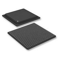
XC6SLX100-2FGG484C Xilinx Inc, XC6SLX100-2FGG484C Datasheet - Page 27

XC6SLX100-2FGG484C
Manufacturer Part Number
XC6SLX100-2FGG484C
Description
FPGA Spartan®-6 Family 101261 Cells 45nm (CMOS) Technology 1.2V 484-Pin FBGA
Manufacturer
Xilinx Inc
Series
Spartan® 6 LXr
Specifications of XC6SLX100-2FGG484C
Package
484FBGA
Family Name
Spartan®-6
Device Logic Cells
101261
Device Logic Units
63288
Number Of Registers
126576
Typical Operating Supply Voltage
1.2 V
Maximum Number Of User I/os
326
Ram Bits
4939776
Number Of Logic Elements/cells
101261
Number Of Labs/clbs
7911
Total Ram Bits
4939776
Number Of I /o
326
Voltage - Supply
1.14 V ~ 1.26 V
Mounting Type
Surface Mount
Operating Temperature
0°C ~ 85°C
Package / Case
484-BBGA
No. Of Logic Blocks
15822
No. Of Macrocells
101261
Family Type
Spartan-6
No. Of Speed Grades
2
No. Of I/o's
326
Clock Management
DCM, PLL
Rohs Compliant
Yes
Lead Free Status / RoHS Status
Lead free / RoHS Compliant
Number Of Gates
-
Lead Free Status / RoHS Status
Lead free / RoHS Compliant
Available stocks
Company
Part Number
Manufacturer
Quantity
Price
Company:
Part Number:
XC6SLX100-2FGG484C
Manufacturer:
ST
Quantity:
4 450
Company:
Part Number:
XC6SLX100-2FGG484C
Manufacturer:
Xilinx Inc
Quantity:
10 000
Output Delay Measurements
Output delays are measured using a Tektronix P6245
TDS500/600 probe (< 1 pF) across approximately 4" of FR4
microstrip trace. Standard termination was used for all
testing. The propagation delay of the 4" trace is
characterized separately and subtracted from the final
measurement, and is therefore not included in the
generalized test setups shown in
X-Ref Target - Figure 4
Table 31: Output Delay Measurement Methodology
DS162 (v2.0) March 31, 2011
Preliminary Product Specification
LVTTL (Low-Voltage Transistor-Transistor Logic)
LVCMOS (Low-Voltage CMOS), 3.3V
LVCMOS, 2.5V
LVCMOS, 1.8V
LVCMOS, 1.5V
LVCMOS, 1.2V
PCI (Peripheral Component Interface)
33 MHz and 66 MHz, 3.3V
HSTL (High-Speed Transceiver Logic), Class I
HSTL, Class II
HSTL, Class III
HSTL, Class I, 1.8V
HSTL, Class II, 1.8V
HSTL, Class III, 1.8V
SSTL (Stub Series Terminated Logic), Class I, 1.8V
SSTL, Class II, 1.8V
SSTL, Class I, 2.5V
FPGA Output
Figure 4: Single-Ended Test Setup
Description
V
REF
R
C
(probe capacitance)
REF
REF
Figure 4
V
(voltage level when taking
delay measurement)
MEAS
ds162_06_011309
and
Figure
5.
www.xilinx.com
Spartan-6 FPGA Data Sheet: DC and Switching Characteristics
LVCMOS33
HSTL_III_18
SSTL18_I
LVTTL (all)
LVCMOS25
LVCMOS18
LVCMOS15
LVCMOS12
PCI33_3, PCI66_3 (rising edge)
PCI33_3, PCI66_3 (falling edge)
HSTL_I
HSTL_II
HSTL_III
HSTL_I_18
HSTL_II_18
SSTL18_II
SSTL2_I
X-Ref Target - Figure 5
Measurements and test conditions are reflected in the IBIS
models except where the IBIS format precludes it.
Parameters V
the test conditions for each I/O standard. The most accurate
prediction of propagation delay in any given application can
be obtained through IBIS simulation, using the following
method:
1. Simulate the output driver of choice into the generalized
2. Record the time to V
3. Simulate the output driver of choice into the actual PCB
4. Record the time to V
5. Compare the results of steps 2 and 4. The increase or
I/O Standard
Attribute
test setup, using values from
trace and load, using the appropriate IBIS model or
capacitance value to represent the load.
decrease in delay yields the actual propagation delay of
the PCB trace.
FPGA Output
Figure 5: Differential Test Setup
REF
, R
REF
, C
C
MEAS
MEAS
R
REF
REF
()
1M
1M
1M
1M
1M
1M
25
25
50
25
50
50
25
50
50
25
50
REF
.
.
, and V
Table
C
(pF)
10
10
REF
0
0
0
0
0
0
0
0
0
0
0
0
0
0
0
(2)
(2)
MEAS
(1)
31.
R
fully describe
REF
V
V
V
V
V
V
V
V
ds162_07_011309
1.65
1.25
0.75
0.75
0.94
2.03
MEAS
(V)
1.1
1.4
0.9
0.9
REF
REF
REF
REF
REF
REF
REF
V
MEAS
+
–
V
0.75
0.75
1.25
(V)
3.3
1.5
0.9
0.9
1.8
0.9
0.9
REF
0
0
0
0
0
0
0
27


