Î Î Î Î Î Î Î Î Î Î Î
Î Î Î Î Î Î Î Î Î Î Î
Î Î Î Î Î Î Î Î Î Î Î
Î Î Î Î Î Î Î Î Î Î Î
Î Î Î Î Î Î Î Î Î Î Î
Î Î Î Î Î Î Î Î Î Î Î
Î Î Î Î Î Î Î Î Î Î Î
Î Î Î Î Î Î Î Î Î Î Î
Î Î Î Î Î Î Î Î Î Î Î
Î Î Î Î Î Î Î Î Î Î Î
Î Î Î Î Î Î Î Î Î Î Î
Î Î Î Î Î Î Î Î Î Î Î
Î Î Î Î Î Î Î Î Î Î Î
Î Î Î Î Î Î Î Î Î Î Î Î Î Î Î Î Î Î Î
Î Î Î Î Î Î Î Î Î Î Î Î Î Î Î Î Î Î Î
Î Î Î Î Î Î Î Î Î Î Î
Î Î Î Î Î Î Î Î Î Î Î
Î Î Î Î Î Î Î Î Î Î Î
Î Î Î Î Î Î Î Î Î Î Î
Î Î Î Î Î Î Î Î Î Î Î
Î Î Î Î Î Î Î Î Î Î Î
Î Î Î Î Î Î Î Î Î Î Î
Î Î Î Î Î Î Î Î Î Î Î Î Î Î Î Î Î Î Î
Î Î Î Î Î Î Î Î Î Î Î Î Î Î Î Î Î Î Î
Î Î Î Î Î Î Î Î Î Î Î
Î Î Î Î Î Î Î Î Î Î Î
Î Î Î Î Î Î Î Î Î Î Î
MJE340
Plastic Medium−Power
NPN Silicon Transistor
Features
•
•
•
Maximum ratings are those values beyond which device damage can occur.
Maximum ratings applied to the device are individual stress limit values (not
normal operating conditions) and are not valid simultaneously. If these limits are
exceeded, device functional operation is not implied, damage may occur and
reliability may be affected.
*For additional information on our Pb−Free strategy and soldering details, please
© Semiconductor Components Industries, LLC, 2006
February, 2006 − Rev. 11
MAXIMUM RATINGS
THERMAL CHARACTERISTICS
ELECTRICAL CHARACTERISTICS
OFF CHARACTERISTICS
ON CHARACTERISTICS
download the ON Semiconductor Soldering and Mounting Techniques
Reference Manual, SOLDERRM/D.
Collector−Emitter Voltage
Emitter−Base Voltage
Collector Current − Continuous
Total Power Dissipation @ T
Operating and Storage Junction
Temperature Range
Thermal Resistance, Junction−to−Case
Collector−Emitter Sustaining Voltage
(I
Collector Cutoff Current
(V
Emitter Cutoff Current
(V
DC Current Gain
(I
This device is useful for high−voltage general purpose applications.
for High Reliability
C
C
Suitable for Transformerless, Line−Operated Equipment
Thermopad Construction Provides High Power Dissipation Rating
Pb−Free Package is Available*
CB
EB
Derate above 25_C
= 1.0 mAdc, I
= 50 mAdc, V
= 3.0 Vdc, I
= 300 Vdc, I
Characteristic
Characteristic
Rating
B
C
CE
E
= 0)
= 0)
= 0)
= 10 Vdc)
C
= 25_C
Î Î Î Î
Î Î Î Î
Î Î Î Î
Î Î Î Î
Î Î Î Î
Î Î Î Î
Î Î Î Î
Î Î Î Î
Î Î Î Î
Î Î Î Î
Î Î Î Î
Î Î Î Î
Î Î Î Î
Î Î Î Î
Î Î Î Î
Î Î Î Î
Î Î Î Î
Î Î Î Î
Î Î Î Î
Î Î Î Î
Î Î Î Î
Î Î Î Î
Î Î Î Î
(T
C
V
Symbol
Symbol
Symbol
CEO(sus)
T
= 25°C unless otherwise noted)
I
I
h
V
CBO
EBO
J
V
q
P
FE
, T
CEO
I
EB
JC
C
D
stg
Î Î Î Î
Î Î Î Î
Î Î Î Î
Î Î Î Î
Î Î Î Î
Î Î Î Î
Î Î Î Î
Î Î Î Î
Î Î Î Î
Î Î Î Î
Î Î Î Î
Î Î Î Î
Î Î Î Î
Î Î
Î Î
Î Î
Î Î Î Î
Î Î
Î Î
Î Î
Î Î Î Î
Min
300
–65 to +150
30
−
−
Î Î Î
Î Î Î
Î Î Î
Î Î Î
Î Î Î
Î Î Î
Î Î Î
Î Î Î
Î Î Î
Î Î Î
Value
0.16
Max
6.25
300
500
3.0
20
Max
100
100
240
−
Î Î Î
Î Î Î
Î Î Î
Î Î Î
Î Î Î
Î Î Î
Î Î Î
Î Î Î
Î Î Î
Î Î Î
Î Î Î
Î Î Î
Î Î Î
Î Î Î
Î Î Î
Î Î Î
Î Î Î
Î Î Î
Î Î Î
Î Î Î
Î Î Î
Î Î Î
Î Î Î
1
mW/_C
mAdc
mAdc
mAdc
_C/W
Unit
Vdc
Unit
Unit
Vdc
Vdc
_C
−
W
MJE340
MJE340G
Device
POWER TRANSISTOR
300 VOLTS, 20 WATTS
3
ORDERING INFORMATION
2 1
Y
WW
JE340 = Device Code
G
MARKING DIAGRAM
http://onsemi.com
NPN SILICON
0.5 AMPERE
(Pb−Free)
= Year
= Work Week
= Pb−Free Package
Package
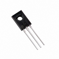
TO−225
TO−225
Publication Order Number:
JE340G
YWW
CASE 77
STYLE 1
TO−225
500 Units/Box
500 Units/Box
Shipping
MJE340/D