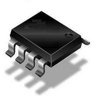
ATA6620N-TASY Atmel, ATA6620N-TASY Datasheet - Page 8

ATA6620N-TASY
Manufacturer Part Number
ATA6620N-TASY
Description
RF Wireless Misc LIN SBC
Manufacturer
Atmel
Datasheet
1.ATA6620N-TAQY.pdf
(22 pages)
Specifications of ATA6620N-TASY
Package / Case
SOIC
Mounting Style
SMD/SMT
Lead Free Status / RoHS Status
Lead free / RoHS Compliant
4.2.2
8
ATA6620N
Sleep Mode
A falling edge at EN while TXD is low switches the IC into Sleep mode. The TXD Signal has to
be logic low during the Mode Select window (see
microcontroller port for EN as for TXD; in this case the mode change is only one command.
In Sleep mode the transmission path is disabled. Supply current from V
I
termination between pin LIN and pin VS is disabled to minimize the power dissipation in case pin
LIN is short-circuited to GND. Only a weak pull-up current (typically 10 µA) between pin LIN and
pin VS is present.
A falling edge at pin LIN followed by a dominant bus level maintained for a certain time period
(t
mode. The V
on. The remote wake-up request is indicated by a low level at pin RXD to interrupt the microcon-
troller and a high level at pin TXD (see
With EN high you can switch directly from Silent to Normal mode. In the application where the
ATA6620N supplies the microcontroller, the wake-up from Sleep mode is only possible via pin
LIN.
If the device is switched into Sleep mode, V
reset at pin NRES.
Figure 4-4.
VSsleep
bus
) results in a remote wake-up request. The device switches from Sleep mode to Pre-normal
= 10 µA. The V
NRES
VCC
TXD
LIN
EN
CC
Normal Mode
Switch to Sleep Mode
regulator is activated and the internal LIN slave termination resistor is switched
CC
t
d
regulator is switched off; NRES and RXD are low. The internal slave
= 3.2 µs
Delay time sleep mode
t
d_sleep
LIN switches directly to recessive mode
Figure 4-5 on page
Mode select window
= maximum 20 µs
CC
ramps down without generating an undervoltage
Figure
4-4). We recommend using the same
9).
Sleep Mode
Batt
4850I–AUTO–09/09
is typically


