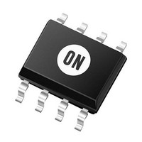
MC12095DR2 ON Semiconductor, MC12095DR2 Datasheet - Page 2

MC12095DR2
Manufacturer Part Number
MC12095DR2
Description
Prescaler 2.5GHz Low Power
Manufacturer
ON Semiconductor
Datasheet
1.MC12095DR2.pdf
(8 pages)
Specifications of MC12095DR2
Division
2/4
Mounting Style
SMD/SMT
Package / Case
SOIC-8
Maximum Operating Frequency
2500 MHz
Minimum Operating Frequency
500 MHz
Supply Voltage (min)
2.7 V
Supply Voltage (max)
5.5 V
Operating Supply Voltage
3.3 V, 5 V
Minimum Operating Temperature
- 40 C
Maximum Operating Temperature
+ 85 C
Lead Free Status / RoHS Status
Lead free / RoHS Compliant
Available stocks
Company
Part Number
Manufacturer
Quantity
Price
Company:
Part Number:
MC12095DR2
Manufacturer:
ON
Quantity:
1 000
Company:
Part Number:
MC12095DR2G
Manufacturer:
TOSHIBA
Quantity:
6 227
Part Number:
MC12095DR2G
Manufacturer:
ON/安森美
Quantity:
20 000
Table 3. MAXIMUM RATINGS
Maximum ratings are those values beyond which device damage can occur. Maximum ratings applied to the device are individual stress limit
values (not normal operating conditions) and are not valid simultaneously. If these limits are exceeded, device functional operation is not implied,
damage may occur and reliability may be affected.
NOTE:
2. JEDEC standard multilayer board − 2S2P (2 signal, 2 power). For DFN8 only, thermal exposed pad must be connected to a sufficient thermal
Table 4. ELECTRICAL CHARACTERISTICS
V
T
T
I
q
f
I
I
V
V
V
V
V
V
O
t
CC
SB
A
stg
JC
CC
IH1
IL1
IH2
IL2
OUT
IN
conduit. Electrically connect to the most negative supply (GND) or leave unconnected, floating open.
Symbol
Symbol
ESD data available upon request.
Power Supply Voltage, Pin 2
Operating Temperature Range
Storage Temperature Range
Maximum Output Current, Pin 4
Thermal Resistance (Junction−to−Case) (Note 2) DFN8
Toggle Frequency (Sine Wave)
Supply Current
Stand−By Current
Stand−By Input HIGH (SB)
Stand−By Input LOW (SB)
Divide Ratio Control Input HIGH (SW)
Divide Ratio Control Input LOW (SW)
Output Voltage Swing (2pF Load)
Input Voltage Sensitivity
Table 2. ATTRIBUTES
1. For additional information, see Application Note AND8003/D.
Internal Input Pulldown Resistor
Internal Input Pullup Resistor
ESD Protection
Moisture Sensitivity, Indefinite Time Out of Drypack (Note 1)
Flammability Rating
Transistor Count
Meets or exceeds JEDEC Spec EIA/JESD78 IC Latchup Test
Characteristic
Characteristics
(V
CC
= 2.7 to 5.5 V; T
Rating
http://onsemi.com
Oxygen Index: 28 to 34
Charged Device Model
1000−1500 MHz Input
1500−2500 MHz Input
500−1000 MHz Input
Human Body Model
Machine Model
2
A
= −40 to 85°C, unless otherwise noted.)
SOIC−8
DFN8
V
CC
OPEN
Pb Pkg
Level 1
Level 1
GND
Min
500
800
400
200
200
UL 94 V−0 @ 0.125 in
2.0
−
−
− 0.4
125 Devices
> 200 V
> 4 kV
> 2 kV
Value
N/A
N/A
OPEN
Pb−Free Pkg
V
Typ
100
450
250
3.0
8.7
−
−
CC
−
−
Level 1
Level 1
−0.5 to 6.0
−65 to 150
−40 to 85
35 to 40
Value
V
V
8.0
CC
CC
OPEN
1000
Max
200
2.5
0.8
14
+ 0.5 V
+ 0.5 V
−
−
−
°C/W
mVpp
mVpp
Unit
Vdc
GHz
mA
Unit
°C
°C
mA
mA
V
V
V


