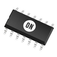
MC1496D ON Semiconductor, MC1496D Datasheet

MC1496D
Specifications of MC1496D
Available stocks
Related parts for MC1496D
MC1496D Summary of contents
Page 1
... These devices were designed for use where the output voltage is a product of an input voltage (signal) and a switching function (carrier). Typical applications include suppressed carrier and amplitude modulation, synchronous detection, FM detection, phase detection, and chopper applications. See ON Semiconductor Application Note AN531 for additional design information. Features • ...
Page 2
I = 500 kHz 1.0 kHz C S Figure 1. Suppressed Carrier Output Waveform I = 500 kHz 1.0 kHz S Figure 3. Amplitude Modulation Output Waveform MAXIMUM RATINGS (T = 25°C, unless otherwise noted.) ...
Page 3
ELECTRICAL CHARACTERISTICS all input and output characteristics are single−ended, unless otherwise noted.) (Note 1) Characteristic Carrier Feedthrough mVrms sine wave and C offset adjusted to zero V = 300 mVpp square wave: C offset adjusted to zero ...
Page 4
Carrier Feedthrough Carrier feedthrough is defined as the output voltage at carrier frequency with only the carrier applied (signal voltage = 0). Carrier null is achieved by balancing the currents in the differential amplifier by means of a bias trim ...
Page 5
Bias currents flowing into Pins and 10 are transistor base currents and can normally be neglected if external bias dividers are designed to carry 1 more. Transadmittance Bandwidth Carrier transadmittance bandwidth is the 3.0 dB ...
Page 6
1 − MC1496 6 −8.0 Vdc V EE Figure 9. Common ...
Page 7
TYPICAL CHARACTERISTICS Typical characteristics were obtained with circuit shown in Figure mVrms 1.0 Signal Port 0.9 0.8 0.7 0.6 Side Band Sideband Transadmittance 0.5 I out (Each Sideband) ⎥ 0 ...
Page 8
CARRIER FREQUENCY (MHz) C Figure 21. Suppression of Carrier Harmonic Sidebands versus Carrier Frequency The MC1496, a monolithic balanced modulator circuit, is shown in Figure 23. ...
Page 9
Table 1. Voltage Gain and Output Frequencies Carrier Input Signal ( Low−level dc High−level dc Low−level ac High−level ac 2. Low−level Modulating Signal assumed in all cases When the output signal contains multiple ...
Page 10
If the carrier signal is modulated, a 300 mVrms input level is recommended. Doubly Balanced Mixer The MC1496 may be used ...
Page 11
Local 3 2 Oscillator 51 8 Input 6 10 0.001 mF 100 mVrms MC1496 1 RF Input 5.0− 6.8 k ...
Page 12
... MC1496BP MC1496BPG †For information on tape and reel specifications, including part orientation and tape sizes, please refer to our Tape and Reel Packaging Specifications Brochure, BRD8011/D. SOIC−14 D SUFFIX CASE 751A 14 14 MC1496DG MC1496BDG AWLYWW 1 1 Package SOIC−14 SOIC−14 (Pb−Free) SOIC−14 SOIC− ...
Page 13
... G −T− SEATING 14 PL PLANE 0.25 (0.010 14X 0.58 *For additional information on our Pb−Free strategy and soldering details, please download the ON Semiconductor Soldering and Mounting Techniques Reference Manual, SOLDERRM/D. PACKAGE DIMENSIONS SOIC−14 CASE 751A−03 ISSUE 0.25 (0.010 ...
Page 14
... 0.13 (0.005 American Technical Support: 800−282−9855 Toll Free USA/Canada Japan: ON Semiconductor, Japan Customer Focus Center 2−9−1 Kamimeguro, Meguro−ku, Tokyo, Japan 153−0051 Phone: 81−3−5773−3850 http://onsemi.com 14 NOTES: 1. DIMENSIONING AND TOLERANCING PER ANSI Y14.5M, 1982. 2. CONTROLLING DIMENSION: INCH. ...


