BCX52,115 NXP Semiconductors, BCX52,115 Datasheet
BCX52,115
Specifications of BCX52,115
BCX52 T/R
BCX52 T/R
Available stocks


Related parts for BCX52,115


BCX52,115 Summary of contents
Page 1
BCP52; BCX52 PNP medium power transistors Rev. 08 — 25 February 2008 1. Product profile 1.1 General description PNP medium power transistor series. Table 1. Type number BCP52 BCX52 [1] Valid for all available selection groups. ...
Page 2
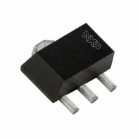
... NXP Semiconductors 2. Pinning information Table 3. Pin SOT223 SOT89 Ordering information Table 4. Type number BCP52 BCX52 [1] Valid for all available selection groups. 4. Marking Table 5. Type number BCP52 BCP52-10 BCP52-16 BCX52 BCX52-10 BCX52-16 BCP52_BCX52_8 Product data sheet Pinning Description base collector emitter collector ...
Page 3
... NXP Semiconductors 5. Limiting values Table 6. In accordance with the Absolute Maximum Rating System (IEC 60134). Symbol V CBO V CEO V EBO tot amb T stg [1] Device mounted on an FR4 Printed-Circuit Board (PCB), single-sided copper, tin-plated and standard footprint. [2] Device mounted on an FR4 PCB, single-sided copper, tin-plated, mounting pad for collector 1 cm ...
Page 4
... NXP Semiconductors 1.6 P tot (W) 1.2 (1) 0.8 (2) 0 (1) FR4 PCB, mounting pad for collector 1 cm (2) FR4 PCB, standard footprint Fig 1. Power derating curves SOT223 6. Thermal characteristics Table 7. Symbol R th(j-a) R th(j-sp) [1] Device mounted on an FR4 PCB, single-sided copper, tin-plated and standard footprint. [2] Device mounted on an FR4 PCB, single-sided copper, tin-plated, mounting pad for collector 1 cm ...
Page 5
... NXP Semiconductors th(j-a) duty cycle = (K/ 0.5 0.33 0.2 0.1 10 0.05 0.02 0. FR4 PCB, standard footprint Fig 3. Transient thermal impedance from junction to ambient as a function of pulse duration for SOT223; typical values 3 10 duty cycle = Z th(j-a) (K/W) 1 0.75 0.5 0.33 0.2 ...
Page 6
... NXP Semiconductors duty cycle = th(j-a) (K/W) 1 0.75 2 0.5 10 0.33 0.2 0.1 0.05 10 0.02 0. FR4 PCB, standard footprint Fig 5. Transient thermal impedance from junction to ambient as a function of pulse duration for SOT89; typical values th(j-a) (K/W) duty cycle = 0.75 0.5 0.33 0.2 0 ...
Page 7
... NXP Semiconductors 3 10 duty cycle = Z th(j-a) (K/W) 1 0.75 0.5 0.33 0.2 10 0.1 0.05 0.02 0. FR4 PCB, mounting pad for collector 6 cm Fig 7. Transient thermal impedance from junction to ambient as a function of pulse duration for SOT89; typical values 7. Characteristics Table unless otherwise specified. ...
Page 8
... NXP Semiconductors 300 ( 200 (2) 100 ( ( 150 C amb ( amb ( amb Fig 8. DC current gain as a function of collector current; typical values 1200 V BE (mV) 1000 (1) 800 (2) 600 (3) 400 200 ( amb ( amb ( 150 C amb Fig 10. Base-emitter voltage as a function of collector current; typical values BCP52_BCX52_8 Product data sheet ...
Page 9
... NXP Semiconductors 8. Package outline 6.7 6.3 3.1 2.9 4 7.3 3.7 6.7 3 2.3 4.6 Dimensions in mm Fig 12. Package outline SOT223 (SC-73) 9. Packing information Table 9. The indicated -xxx are the last three digits of the 12NC ordering code. Type number BCP52 BCX52 [1] For further information and the availability of packing methods, see [2] Valid for all available selection groups ...
Page 10
... NXP Semiconductors 10. Revision history Table 10. Revision history Document ID Release date BCP52_BCX52_8 20080225 • Modifications: • BC638_BCP52_BCX52_7 20070626 BC638_BCP52_BCX52_6 20060329 BC636_638_640_5 20041011 BCP51_52_53_5 20030206 BCX51_52_53_4 20011010 BCP52_BCX52_8 Product data sheet Data sheet status Product data sheet Type numbers BC638 and BC638-16 have been removed ...
Page 11
... Right to make changes — NXP Semiconductors reserves the right to make changes to information published in this document, including without limitation specifications and product descriptions, at any time and without notice ...
Page 12
... NXP Semiconductors 13. Contents 1 Product profi 1.1 General description 1.2 Features . . . . . . . . . . . . . . . . . . . . . . . . . . . . . . 1 1.3 Applications . . . . . . . . . . . . . . . . . . . . . . . . . . . 1 1.4 Quick reference data Pinning information . . . . . . . . . . . . . . . . . . . . . . 2 3 Ordering information . . . . . . . . . . . . . . . . . . . . . 2 4 Marking . . . . . . . . . . . . . . . . . . . . . . . . . . . . . . . . 2 5 Limiting values Thermal characteristics Characteristics . . . . . . . . . . . . . . . . . . . . . . . . . . 7 8 Package outline . . . . . . . . . . . . . . . . . . . . . . . . . 9 9 Packing information Revision history . . . . . . . . . . . . . . . . . . . . . . . . 10 11 Legal information ...