PZT3906T1 ON Semiconductor, PZT3906T1 Datasheet

TRANS SS GP PNP 200MA 40V SOT223

PZT3906T1

Manufacturer Part Number
PZT3906T1
Description
TRANS SS GP PNP 200MA 40V SOT223
Manufacturer
ON Semiconductor
Datasheet

Specifications of PZT3906T1

Transistor Type
PNP
Current - Collector (ic) (max)
200mA
Voltage - Collector Emitter Breakdown (max)
40V
Vce Saturation (max) @ Ib, Ic
400mV @ 5mA, 50mA
Dc Current Gain (hfe) (min) @ Ic, Vce
100 @ 10mA, 1V
Power - Max
1.5W
Frequency - Transition
250MHz
Mounting Type
Surface Mount
Package / Case
SOT-223 (3 leads + Tab), SC-73, TO-261
Lead Free Status / RoHS Status
Contains lead / RoHS non-compliant
Current - Collector Cutoff (max)
-
Other names
PZT3906T1OS
PZT3906T1
General Purpose Transistor
PNP Silicon
Features
Stresses exceeding Maximum Ratings may damage the device. Maximum
Ratings are stress ratings only. Functional operation above the Recommended
Operating Conditions is not implied. Extended exposure to stresses above the
Recommended Operating Conditions may affect device reliability.
1. FR−4 with 1 oz and 713 mm
© Semiconductor Components Industries, LLC, 2006
March, 2006 − Rev. 2
MAXIMUM RATINGS
THERMAL CHARACTERISTICS
Collector −Emitter Voltage
Collector −Base Voltage
Emitter −Base Voltage
Collector Current − Continuous
Total Device Dissipation (Note 1)
Thermal Resistance Junction−to−Ambient
Thermal Resistance Junction−to−Lead #4
Junction and Storage Temperature Range
Pb−Free Package is Available
T
(Note 1)
A
= 25°C
Characteristic
Rating
Preferred Device
2
of copper area.
Symbol
Symbol
T
V
V
V
R
R
J
P
CEO
CBO
EBO
, T
I
qJA
qJA
C
D
stg
−55 to
Value
−200
+150
−5.0
Max
83.3
−40
−40
1.5
12
35
1
mW/°C
mAdc
°C/W
°C/W
Unit
Unit
Vdc
Vdc
Vdc
°C
W
†For information on tape and reel specifications,
Preferred devices are recommended choices for future use
and best overall value.
PZT3906T1
PZT3906T1G
including part orientation and tape sizes, please
refer to our Tape and Reel Packaging Specifications
Brochure, BRD8011/D.
Device
(Note: Microdot may be in either location)
BASE
ORDERING INFORMATION
2A
A
Y
W
G
1
http://onsemi.com
(Pb−Free)
SOT−223
SOT−223
Package
COLLECTOR
= Specific Device Code
= Assembly Location
= Year
= Work Week
= Pb−Free Package
EMITTER
2, 4
Publication Order Number:
3
1
1000 / Tape & Reel
1000 / Tape & Reel
MARKING
DIAGRAM
Shipping
AYW
PZT3906T1/D
2A G
G

Related parts for PZT3906T1

PZT3906T1 Summary of contents

Page 1

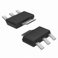
... DIAGRAM AYW Specific Device Code A = Assembly Location Y = Year W = Work Week G = Pb−Free Package (Note: Microdot may be in either location) ORDERING INFORMATION † Package Shipping SOT−223 1000 / Tape & Reel SOT−223 1000 / Tape & Reel (Pb−Free) Publication Order Number: PZT3906T1/D ...

Page 2

ELECTRICAL CHARACTERISTICS Characteristic OFF CHARACTERISTICS (Note 2) Collector −Emitter Breakdown Voltage (Note −1.0 mAdc Collector −Base Breakdown Voltage (I = −10 mAdc Emitter −Base Breakdown Voltage (I ...

Page 3

10.6 V 300 ns DUTY CYCLE = 2% Figure 1. Delay and Rise Time Equivalent Test Circuit 3 V +9.1 V 275 0 C < 4 pF* S < 500 ms 10 < ...

Page 4

TYPICAL TRANSIENT CHARACTERISTICS 10 7.0 5.0 C obo C ibo 3.0 2.0 1.0 0.1 0.2 0.3 0.5 0.7 1.0 2.0 3.0 5.0 7.0 10 REVERSE BIAS (VOLTS) Figure 3. Capacitance 500 300 200 100 ...

Page 5

I , COLLECTOR CURRENT (mA) C Figure 9. Current Gain 20 10 7.0 5.0 3.0 2.0 1.0 0.7 0.5 0.3 0.2 0.1 0.2 0.3 0.5 0.7 1.0 ...

Page 6

TYPICAL STATIC CHARACTERISTICS 2.0 1.0 0.7 0.5 0.3 0.2 0.1 0.1 0.2 0.3 0.5 0.7 1.0 1 0.6 0.4 0.2 0 0.01 0.02 0.03 0.05 0.07 1 25° ...

Page 7

... PIN 1. BASE 2. COLLECTOR 3. EMITTER 4. COLLECTOR ON Semiconductor Website: http://onsemi.com Order Literature: http://www.onsemi.com/litorder For additional information, please contact your local Sales Representative. PZT3906T1/D MAX 0.068 0.004 0.035 0.126 0.014 0.263 0.145 0.094 0.041 0.078 0.287 10° ...

Related keywords