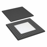
AD8152JBP Analog Devices Inc, AD8152JBP Datasheet - Page 23

AD8152JBP
Manufacturer Part Number
AD8152JBP
Description
Digital Crosspoint 34 x 34 X-Point SW 3.2Gbps 256-Pin SBGA
Manufacturer
Analog Devices Inc
Datasheet
1.AD8152JBPZ.pdf
(32 pages)
Specifications of AD8152JBP
Package
256SBGA
Array Configuration
34x34
Number Of Arrays
1
Maximum Data Rate
3.2 Gbps
Power Supply Type
Single
Minimum Single Supply Voltage
2.25 V
Maximum Single Supply Voltage
3.63 V
Rohs Status
RoHS non-compliant
Function
Crosspoint Switch
Circuit
1 x 34:34
Voltage Supply Source
Single Supply
Voltage - Supply, Single/dual (±)
2.5 V ~ 3.3 V
Current - Supply
32mA
Operating Temperature
0°C ~ 85°C
Mounting Type
Surface Mount
Package / Case
256-BGA Exposed Pad, 256-eBGA, 256-HBGA
Lead Free Status / RoHS Status
Available stocks
Company
Part Number
Manufacturer
Quantity
Price
Company:
Part Number:
AD8152JBP
Manufacturer:
ADI
Quantity:
170
Company:
Part Number:
AD8152JBP
Manufacturer:
Analog Devices Inc
Quantity:
10 000
Company:
Part Number:
AD8152JBPZ
Manufacturer:
ADI
Quantity:
642
Company:
Part Number:
AD8152JBPZ
Manufacturer:
Analog Devices Inc
Quantity:
10 000
Connections for Testing
The AD8152 evaluation board can be used under a variety of posi-
tive or negative supply configurations. Negative supply configurations,
as shown in Figure 15, allow the easiest hookup to test equip-
ment because inputs and outputs can be direct coupled. In a real
world application however, the negative supply configuration would
be difficult because control logic levels must be shifted negative.
Figure 16 is an example of a loop-through test setup using a posi-
tive supply. In this case, the test signal goes through the AD8152
twice. It is possible to loop through multiple times if desired, but
jitter will increase with number of loop-throughs. The first
input from the generator and the last output to a scope must be
ac-coupled. However, an AD8152 output driving its own input can
be direct-coupled. Direct coupling to the first AD8152 input is not
effective since generators usually want to see 50 W to ground.
REV. A
Figure 15. Evaluation Board ECL Driver Test Setup
TRIGGER OUT
GENERATOR
PATTERN
DRIVER
ECL
DATA OUT
DATA OUT
VTTI = –2V
N
P
IN
AD8152
–6dB
–6dB
VCC
Figure 16. Positive Supply Loop-Through Test Setup
OUT
VCC = VTTI = VTTO = 2.5V, VEE = 0V, I
RTI (REFERRED TO INPUT) A MPLITUDE = 400mV SINGLE–ENDED,
V
V
AC-COUPLED IS FROM BIAS TEES,
PROGRAMMING: IN01 TO OUT02, IN02 TO OUT01.
IN
OL
N
VTTO
P
HI = 2.7V (IN01), PRBS 2
= 2.1V,
VEE = –2.5V
TO 50
INPUTS
SCOPE
VTTI
2.5V
IN01
IN02
P
N
N
P
AD8152
23
VEE
–1, V
–23–
VCC
OH
OUT01
OUT02
OUT
= 2.5V,
This would require VTTI to be attached to ground, causing
excessive power to be dissipated in the internal 50 W input
termination resistors. Secondly, when the AD8152 output tries
to drive its own input with VTTI = 0 V and VTTO = 2.5 V, the
input will pull the output stage levels down enough to shut off
any signal toggling.
All ac coupling shown is actually done with a set of bias tees. If
desired, the bias tee can be used to monitor average dc voltage
levels at an input or output (depending on direction installed),
and it can also serve to change input dc levels. Make sure the
bias tees used in the setup have enough low frequency bandwidth
to pass long patterns and keep edge rates intact. The longer the
pattern, the more low frequency bandwidth is needed.
If ac coupling is desired on a user board, 0402 or 0603 sized
capacitors can be installed on microstrip lines. The biggest 0402
size, XR7 type usable is 0.01 mF, which will work fine for short
patterns (PRBS 2
long patterns a 0603 sized, XR7 type, 0.1 mF should be used. To
decrease capacitive loading from the mounting area, clear out
planes underneath the coupling capacitor.
In Figure 16, 6 dB attenuators are placed before the AD8152
input ac-coupling or bias tees. This is because many generators
won’t go below 500 mV single-ended. The output pair of 6 dB
attenuators is present to protect the scope inputs and allow for
higher scale voltages per division. The eye diagram is usually
viewed differentially by using a simple P – N math function.
Cabling used in this setup must be matched. Mismatched cables
cause either a P or N signal to be falsely delayed. This delay can
show up as a change in the crossing point, from 50 percent in the
eye diagram. To accurately check cable matches, a TDR setup
is recommended.
N
N
P
P
VTTO
SET = 16mA
7
–1) and data rates down to 1.0 Gbps. For
–6dB
–6dB
OSCILLOSCOPE
HIGH SPEED
50
50
SAMPLING
TRIGGER IN
AD8152


