DTA144TT1 ON Semiconductor, DTA144TT1 Datasheet

TRANS PNP BIAS RES 50V SC-59

DTA144TT1

Manufacturer Part Number
DTA144TT1
Description
TRANS PNP BIAS RES 50V SC-59
Manufacturer
ON Semiconductor
Datasheet

Specifications of DTA144TT1

Transistor Type
PNP - Pre-Biased
Current - Collector (ic) (max)
100mA
Voltage - Collector Emitter Breakdown (max)
50V
Resistor - Base (r1) (ohms)
47K
Dc Current Gain (hfe) (min) @ Ic, Vce
160 @ 5mA, 10V
Vce Saturation (max) @ Ib, Ic
250mV @ 1mA, 10mA
Current - Collector Cutoff (max)
500nA
Power - Max
230mW
Mounting Type
Surface Mount
Package / Case
SC-59-3, SMT3, SOT-346, TO-236
Lead Free Status / RoHS Status
Contains lead / RoHS non-compliant
Other names
DTA144TT1OS
PNP Silicon Surface Mount Transistor
with Monolithic Bias Resistor Network
device and its external resistor bias network. The BRT (Bias Resistor
Transistor) contains a single transistor with a monolithic bias network
consisting of two resistors; a series base resistor and a base–emitter
resistor. The BRT eliminates these individual components by
integrating them into a single device. The use of a BRT can reduce
both system cost and board space. The device is housed in the SC–59
package which is designed for low power surface mount applications.
1. FR–4 @ Minimum Pad
2. FR–4 @ 1.0 x 1.0 inch Pad
MAXIMUM RATINGS
May, 2002 – Rev. 1
THERMAL CHARACTERISTICS
DEVICE MARKING AND RESISTOR VALUES
Collector-Base Voltage
Collector-Emitter Voltage
Collector Current
Total Device Dissipation
Derate above 25 C
Thermal Resistance –
Junction and Storage
This new series of digital transistors is designed to replace a single
ESD Rating
The modified gull–winged leads absorb thermal stress during
soldering eliminating the possibility of damage to the die.
Use the Device Number to order the 7 inch/3000 unit reel.
Simplifies Circuit Design
Reduces Board Space
Reduces Component Count
Moisture Sensitivity Level: 1
ESD Rating – Human Body Model: Class 1
The SC–59 package can be soldered using wave or reflow.
Available in 8 mm embossed tape and reel
Semiconductor Components Industries, LLC, 2002
DTA144TT1
T
Junction-to-Ambient
Junction-to-Lead
Temperature Range
A
Device
= 25 C
Characteristic
Rating
– Machine Model: Class B
Marking
(T
6T
A
= 25 C unless otherwise noted)
Preferred Device
R1 (K)
47
Symbol
Symbol
T
V
V
R
R
J
P
CBO
CEO
, T
I
C
D
JA
JL
stg
R2 (K)
230 (Note 1.)
338 (Note 2.)
540 (Note 1.)
370 (Note 2.)
264 (Note 1.)
287 (Note 2.)
1.8 (Note 1.)
2.7 (Note 2.)
–55 to +150
Value
Max
100
50
50
3000/Tape & Reel
Shipping
1
mAdc
Unit
Unit
Vdc
Vdc
mW
C/W
C/W
C/W
C
Preferred devices are recommended choices for future use
and best overall value.
DTA144TT1
Device
PIN 1
BASE
(INPUT)
ORDERING INFORMATION
BIAS RESISTOR
6T = Specific Device Code
M = Date Code
MARKING DIAGRAM
http://onsemi.com
PNP SILICON
TRANSISTOR
R1
R2
Package
CASE 318D
SC–59
1
PLASTIC
SC–59
6T M
2
Publication Order Number:
3
PIN 2
EMITTER
(GROUND)
PIN 3
COLLECTOR
(OUTPUT)
3000/Tape & Reel
Shipping
DTA144TT1/D

Related parts for DTA144TT1

DTA144TT1 Summary of contents

Page 1

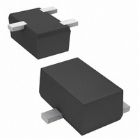
... PIN 2 EMITTER (GROUND SC–59 CASE 318D PLASTIC MARKING DIAGRAM Specific Device Code M = Date Code ORDERING INFORMATION Device Package Shipping DTA144TT1 SC–59 3000/Tape & Reel Preferred devices are recommended choices for future use and best overall value. Publication Order Number: DTA144TT1/D ...

Page 2

... I = 1.0 mA Output Voltage ( Output Voltage (off Input Resistor 1. Pulse Test: Pulse Width < 300 s, Duty Cycle < 2.0% 350 300 250 200 150 100 50 0 –50 DTA144TT1 ( unless otherwise noted) A Symbol I CBO I CEO I EBO V (BR)CBO V (BR)CEO CE(sat 370 C 100 T ...

Page 3

... When using infrared heating with the reflow soldering method, the difference should be a maximum DTA144TT1 interface between the board and the package. With the correct pad geometry, the packages will self align when subjected to a solder reflow process. ...

Page 4

... This profile shows temperature versus time. DTA144TT1 SOLDER STENCIL GUIDELINES The stencil opening size for the surface mounted package should be the same as the pad size on the printed circuit board, i ...

Page 5

... DTA144TT1 PACKAGE DIMENSIONS CASE 318D– http://onsemi.com SC–59 ISSUE ...

Page 6

... Notes DTA144TT1 http://onsemi.com 6 ...

Page 7

... Notes DTA144TT1 http://onsemi.com 7 ...

Page 8

... N. American Technical Support: 800–282–9855 Toll Free USA/Canada DTA144TT1 JAPAN: ON Semiconductor, Japan Customer Focus Center 4–32–1 Nishi–Gotanda, Shinagawa–ku, Tokyo, Japan 141–0031 Phone: 81–3–5740–2700 Email: r14525@onsemi.com ON Semiconductor Website: http://onsemi.com For additional information, please contact your local Sales Representative. http://onsemi.com 8 DTA144TT1/D ...

Related keywords