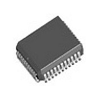
DG884AM883E3 Vishay, DG884AM883E3 Datasheet - Page 10

DG884AM883E3
Manufacturer Part Number
DG884AM883E3
Description
Manufacturer
Vishay
Datasheet
1.DG884AM883E3.pdf
(23 pages)
Specifications of DG884AM883E3
Array Configuration
8x4
Number Of Arrays
1
Screening Level
Industrial
Pin Count
44
Package Type
PLCC
Power Supply Requirement
Triple
Lead Free Status / RoHS Status
Compliant
DG884
Vishay Siliconix
DEVICE DESCRIPTION
The DG884 is the world’s first monolithic wideband
crosspoint array that operates from dc to > 100 MHz. The
DG884 offers the ability to route any one of eight input
signals to any one of four OUT pins. Any input can be routed
to one, two, three or four OUTs simultaneously with no risk
of shorting inputs together (guaranteed by design).
Each crosspoint is configured as a “T” switch in which DMOS
FETs are used due to their excellent low resistance and low
capacitance characteristics. Each OUT line has a series
switch that minimizes capacitive loading when the OUT is off.
Interfacing
The DG884 was designed to allow complex matrices to be
developed while maintaining a simple control interface. The
status of the I/O pin determines whether the DG884 is being
written to or read from (see Figures 1 and 2).
In order to WRITE to an individual latch, CS and I/O need to
be low, while RS, WR and SALVO must be high. The IN to
OUT path is selected by using address A
define the IN line and address B
line. That is, The IN defined by A
connected to the OUT defined by B
loaded into the Next Event latches when WR goes low and
returns high again. This operation is repeated up to three
more times if other crosspoint connections need to be
changed.
www.vishay.com
10
5, 7, 9, 11, 13, 15, 17, 19
1, 3, 4, 6, 8, 10, 12, 14,
PIN DESCRIPTION
16, 18, 20, 41, 43
31, 32, 33, 34
22, 23, 24, 25
2, 40, 42, 44
27, 28
Pin
39
26
21
38
29
30
35
36
37
OUT
A
DIS
0
IN
, A
Symbol
SALVO
DGND
B
GND
1
1
1
0
WR
I/O
CS
1
0
RS
V+
V
0
V-
to IN
to OUT
to DIS
, A
, B
and B
0
L
through A
, B
2
1
, A
8
1
4
. This chosen path is
3
1
4
to define the OUT
0
3
through A
Analog Signal Ground
Digital Ground
Positive Supply Voltage
Negative Supply Voltage
Logic Supply Voltage - generally 5 V
8 Analog Input Channels
4 Analog Output Channels
Determines whether data is being written into the Next Event latches or read from the
Current Event latches
Chip Select - a logic input
IN Address - logic inputs or outputs as defined by I/O pin, select one of eight IN channels
OUT Address - logic inputs, select one of four OUT channels
Write command that latches A
Master write command, that in one action, transfers all the data from Next Event latches
into Current Event latches
Reset - a low will clear the Current Event latches
Open drain disable outputs - these outputs pull low when the corresponding OUT channel
is off
is electrically
3
to
Upon completing all crosspoint connections that are to be
changed in a single device, other DG884s can be similarly
preset by taking the CS pin low on the appropriate device.
When all DG884s are preset, the Current Event latches are
simultaneously changed by a single SALVO command
applied to all devices. In this manner the crosspoint
configuration
simultaneously updated.
DIS Outputs
Four open drain disable OUTs are provided to control
external line drivers or to provide visual or electrical
signaling. For example, any or all of the DIS OUTs can
directly interface with a CLC410 Video Amplifier to place it
into a high impedance, low-power standby mode when the
corresponding OUT is not being used. (See Figure 15). The
DIS outputs are low and sink to V- when corresponding OUT
is open or RS is low.
Reset
The reset function (RS) allows the resetting of all crosspoints
to a known state (open). At power up, the reset facility may
be used to guarantee that all switches are open. It should be
noted that RS clears the Current Event latches, but the Next
Event latches remain unchanged. This useful facility allows
the user to return the matrix to its previous state (prior to
reset)
Alternatively, the user can reprogram the Next Event latches,
and then apply the SALVO command to reconfigure the
matrix to a new state.
0
, A
by
1
, A
simply
2
Description
, A
of
3
into the Next Event latches
any
applying
number
the
S-71241–Rev. H, 25-Jun-07
Document Number: 70071
of
SALVO
devices
command.
can
be


