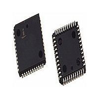
CD22M3494MQAZ Intersil, CD22M3494MQAZ Datasheet - Page 3

CD22M3494MQAZ
Manufacturer Part Number
CD22M3494MQAZ
Description
Manufacturer
Intersil
Datasheet
1.CD22M3494MQAZ.pdf
(8 pages)
Specifications of CD22M3494MQAZ
Array Configuration
16x8
Number Of Arrays
1
Screening Level
Industrial
Pin Count
44
Package Type
PLCC
Power Supply Requirement
Single
Lead Free Status / RoHS Status
Compliant
Available stocks
Company
Part Number
Manufacturer
Quantity
Price
Company:
Part Number:
CD22M3494MQAZ96
Manufacturer:
PANASONIC
Quantity:
34 000
Part Number:
CD22M3494MQAZ96
Manufacturer:
INTERSIL
Quantity:
20 000
Absolute Maximum Ratings
DC Supply Voltage (V
DC Supply Voltage (V
DC Input Diode Current, I
DC Output Diode Current, I
DC Transmission Gate Current . . . . . . . . . . . . . . . . . . . . . . . . . . ±25mA
Power Dissipation Per Package (Po)
For T
CAUTION: Stresses above those listed in “Absolute Maximum Ratings” may cause permanent damage to the device. This is a stress only rating and operation of the
device at these or any other conditions above those indicated in the operational sections of this specification is not implied.
NOTE:
Electrical Specifications
Electrical Specifications
STATIC CONTROLS
Supply Current
High-Level Input Voltage
Low-Level Input Voltage
Input Leakage Current, Digital
STATIC CROSSPOINTS
ON Resistance
ON Resistance
Difference in ON Resistance
Between Any Two Switches
1. θ
Voltages Referenced to V
Voltages Referenced to V
For V
Analog < V
For V
Analog < V
For T
For T
A
JA
A
= -40°C to 85°C (PLCC) . . . . . . . . . . . . . . . . . . . . . . .600mW
I
O
A
, Digital < V
is measured with the component mounted on an evaluation PC board in free air.
, Digital < V
= 60°C to 85°C Derate Linearly . . . . . . .12mW/°C to 200mW
= -40°C to 85°C (PDIP). . . . . . . . . . . . . . . . . . . . . .500mW
PARAMETER
PARAMETER
EE
EE
-0.5V or V
-0.5V or V
SS
SS
DD
DD
-0.5V or V
-0.5V or V
)
)
IN
I
O
> V
OK
EE
SS
> V
DD
DD
. . . . . . . . . . . . . . . . . . . . -0.5 to 16V
. . . . . . . . . . . . . . . . . . . . . -0.5, 16V
I
,
O
3
0.5V. . . . . . . . . . . . . . . . . . . . ±20mA
,
0.5V . . . . . . . . . . . . . . . . . . . ±20mA
T
T
A
A
= -40°C to 85°C, V
= -40°C to 85°C, V
SYMBOL
SYMBOL
∆r
I
V
r
r
V
I
DD
ON
ON
IN
ON
IH
IL
V
V
V
Reset = Low (Note 3)
V
T
- VY = 0.2V
T
V
V
T
V
A
A
A
DD
DD
DD
SS
IN
SS
SS
= 25°C, V
= -40°C to 85°C,
= 25°C, V
= V
DD
= V
= V
= V
= 5V, Logic Inputs = V
= 15V, Logic Inputs = V
= 5V
DD
DD
= 12V, V
EE
EE
EE
= 5V, V
/2, VX -VY = 0.2V,
CD22M3494
TEST CONDITIONS
= 0V,
= 0V
= 0V, V
TEST CONDITIONS
IN
IN
= V
= V
SS
SS
DD
DD
DD
= 0V, V
= 0V, V
/2, VX
/2, VX - VY = 0.2V,
= 12V
Thermal Information
Thermal Resistance (Typical, Note 1)
Maximum Junction Temperature Plastic Package . . . . . . . . . . 150°C
Maximum Storage Temperature Range (T
Maximum Lead Temperature (Soldering 10s) . . . . . . . . . . . . . 300°C
*Pb-free PDIPs can be used for through hole wave solder processing
only. They are not intended for use in Reflow solder processing.
applications.
Operating Conditions
Operating Temperature Range (T
Supply Voltage Range
DC Input or Output Voltage V
Digital Input Voltage. . . . . . . . . . . . . . . . . . . . . . . . . . . . V
EE
EE
DD
PDIP Package* . . . . . . . . . . . . . . . . . . . . . . . . . . . .
PLCC Package. . . . . . . . . . . . . . . . . . . . . . . . . . . . .
Package Type E and Q . . . . . . . . . . . . . . . . . . . . . . -40°C to 85°C
For T
DD
(PLCC - Lead Tips Only)
V
= 0V, Unless Otherwise Specified.
SS
= 0V, Unless Otherwise Specified
V
V
V
V
DD
DD
DD
DD
A
= 0V, V
= Full Package Temperature Range
= 10V
= 10V
= 12V
= 12V
EE
= 0V, V
(Note 2)
MIN
2.4
MIN
-
-
-
-
DD
-
-
-
-
-
. . . . . . . . . . . . . . . . . . . . . . . 4V to 15V
I
or V
A
)
O
TYP
TYP
. . . . . . . . . . . . . . . V
-
-
-
-
-
40
36
50
45
6
STG
). . . . . -65°C to 150°C
(Note 2)
(Note 4)
MAX
MAX
±10
0.8
2
5
75
65
75
65
10
-
January 16, 2006
θ
JA
EE
SS
UNITS
UNITS
FN2793.7
(°C/W)
55
43
mA
mA
to V
to V
µA
Ω
Ω
Ω
Ω
Ω
V
V
DD
DD


