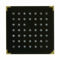
XCF08PFSG48C Xilinx Inc, XCF08PFSG48C Datasheet - Page 32

XCF08PFSG48C
Manufacturer Part Number
XCF08PFSG48C
Description
PROM, PLATFORM FLASH, 8MBIT, 48TFBGA
Manufacturer
Xilinx Inc
Datasheet
1.XCF01SVOG20C.pdf
(35 pages)
Specifications of XCF08PFSG48C
Memory Type
Flash
Memory Size
8Mbit
Clock Frequency
50MHz
Memory Case Style
BGA
No. Of Pins
48
Operating Temperature Range
-40°C To +85°C
Programmable Type
In System Programmable
Voltage - Supply
1.65 V ~ 2 V
Operating Temperature
-40°C ~ 85°C
Package / Case
48-BFBGA, CSPBGA
Interface Type
Serial, Parallel, JTAG
Supply Voltage Range
1.65V To 2V
Rohs Compliant
Yes
Lead Free Status / RoHS Status
Lead free / RoHS Compliant
Other names
122-1453
Available stocks
Company
Part Number
Manufacturer
Quantity
Price
Company:
Part Number:
XCF08PFSG48C
Manufacturer:
SY
Quantity:
1 200
Company:
Part Number:
XCF08PFSG48C
Manufacturer:
XILINX
Quantity:
465
Revision History
The following table shows the revision history for this document.
DS123 (v2.18) May 19, 2010
Product Specification
04/29/03
06/03/03
11/05/03
11/18/03
12/15/03
05/07/04
Date
R
Version
1.0
1.1
2.0
2.1
2.2
2.3
Xilinx Initial Release.
Made edits to all pages.
Major revision.
Pinout corrections as follows:
•
•
•
• Added specification (4.7kΩ) for recommended pull-up resistor on OE/RESET pin to section
• Added paragraph to section
• Section
• Section
•
• Section
• Section
•
• Section
•
• Section
• Section
• Section
• (Continued on next page)
• Section
• Section
• Section
•
Table
• For VO48 package, removed 38 from VCCINT and added it to VCCO.
• For FS48 package, removed pin D6 from VCCINT and added it to VCCO.
Table 14
• For pin D6, changed name from VCCINT to VCCO.
• For pin A4, changed name from GND to DNC.
Figure 8
"Reset and Power-On Reset Activation," page
and/or buffer on the DONE pin.
itemized features.
descriptive text.
Table 2, page
to tie CF High if it is not tied to the FPGA’s PROG_B (PROGRAM) input.
Figure 6, page
CF pin in each configuration.
Table 12, page
the Low state of CF.
• Revised footnote callout number on T
• Added Footnote (2) callout to T
• Added Typical (Typ) parameter columns and parameters for V
• Added 1.5V operation parameter row to V
• Revised V
• Added parameter row T
• Added parameter row and parameters for parallel configuration mode, ’P’ devices, to I
• Added Footnote (1) and Footnote (2) with callouts in the Test Conditions column for I
• Corrected description for second T
• Revised Footnote (7) to indicate V
• Applied Footnote (7) to second T
Footnote (5)T
Table 14, page
• Added additional state conditions to CLK description.
• Added function of resetting the internal address counter to CF description.
I
CCINTS
13:
"Initiating FPGA Configuration," page 10
"Features," page
"Description," page 1
"Design Revisioning," page
"I/O Input Voltage Tolerance and Power Sequencing," page
"Absolute Maximum Ratings," page
"Supply Voltage Requirements for Power-On Reset and Power-Down," page
"Recommended Operating Conditions," page
"DC Characteristics Over Operating Conditions," page
"AC Characteristics Over Operating Conditions," page
"AC Characteristics Over Operating Conditions When Cascading," page
(VO48 package): For pin 38, changed name from VCCINT to VCCO.
(FS48 package):
, I
CCOS
IH
CYC
3: Updated Virtex®-II configuration bitstream sizes.
16, through
25: Added CF column to truth table, and added an additional row to document
39:
Min, 2.5V operation, from 2.0V to 1.7V.
, and I
Min and T
www.xilinx.com
Platform Flash In-System Programmable Configuration PROMs
CCJS
1: Added package styles and 33 MHz configuration speed limit to
IN
Figure 13, page
CAC
"Standby Mode," page
, to define active and standby mode requirements.
and Max parameters
and following: Added state conditions for CF and BUSY to the
Min formulas.
VCC
CYC
8: Rewritten.
CCO
CAC
.
OER
parameter line.
Revision
= 3.3V.
parameter line to show parameters for 1.8V V
23: Added footnote indicating the directionality of the
13: Revised V
IL
from Footnote (4) to Footnote (3).
11.
and V
and following, five instances: Added instruction
12, concerning use of a pull-up resistor
IH
14:
, ’P’ devices.
IN
and V
16:
15:
CCINT
TS
11: Rewritten.
for ’P’ devices.
and V
CCO
/V
23: Revised
CCJ
13:
.
CCJ
CCO
CCO
,
.
.
32


