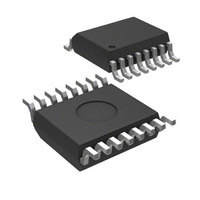
MIC2583-MBQS Micrel Inc, MIC2583-MBQS Datasheet - Page 16

MIC2583-MBQS
Manufacturer Part Number
MIC2583-MBQS
Description
IC,Power Control/Management,CMOS,SSOP,16PIN,PLASTIC
Manufacturer
Micrel Inc
Type
Hot-Swap Controllerr
Datasheet
1.MIC2582-JYM.pdf
(25 pages)
Specifications of MIC2583-MBQS
Applications
General Purpose
Internal Switch(s)
No
Voltage - Supply
2.3 V ~ 13.2 V
Operating Temperature
-40°C ~ 85°C
Mounting Type
Surface Mount
Package / Case
16-SSOP (0.150", 3.90mm Width)
Linear Misc Type
Positive Low Voltage
Family Name
MIC2583
Package Type
QSOP
Operating Supply Voltage (min)
2.3V
Operating Supply Voltage (max)
13.2V
Operating Temperature (min)
-40C
Operating Temperature (max)
85C
Operating Temperature Classification
Industrial
Product Depth (mm)
3.99mm
Product Height (mm)
1.4mm
Product Length (mm)
4.98mm
Mounting
Surface Mount
Pin Count
16
Lead Free Status / RoHS Status
Contains lead / RoHS non-compliant
Lead Free Status / RoHS Status
Contains lead / RoHS non-compliant
Application Information
Design Consideration for Output Undervoltage
Detection
For output undervoltage detection, the first consideration
is to establish the output voltage level that indicates
“power is good.” For this example, the output value for
which a 12V supply will signal “good” is 11V. Next,
consider the tolerances of the input supply and FB
threshold (V
±5%, thus the resulting output voltage may be as low as
11.4V and as high as 12.6V. Additionally, the FB
threshold has ±50mV tolerance and may be as low as
1.19V and as high as 1.29V. Thus, to determine the
values of the resistive divider network (R5 and R6) at the
FB pin, shown in the typical application circuit on page 1,
use the following iterative design procedure.
Using some basic algebra and simplifying Equation 9 to
isolate R5, yields:
Micrel, Inc.
April 2009
1) Choose R6 to allow 100µA or more in the FB
2) Next, determine R5 using the output “good”
resistive divider branch.
R6 is chosen as 12.4kΩ ±1%.
voltage of 11V and the following equation:
V
R
OUT(Good)
6
=
FB
). For this example, the 12V supply varies
V
100
FB(MAX)
μ
=
A
V
FB
=
⎡
⎢
⎣
100
1.29V
(
R5
μ
R6
+
A
R6
=
Figure 6. PCB Connection Sense with ON/OFF Control
)
12
⎤
⎥
⎦
.
9
kΩ
(9)
16
where V
12.4kΩ. Substituting these values into Equation 9.1 now
yields R5 = 93.33kΩ. A standard 93.1kΩ ±% is selected.
Now, consider the 11.4V minimum output voltage, the
lower tolerance for R6 and higher tolerance for R5,
12.28kΩ and 94.03kΩ, respectively. With only 11.4V
available, the voltage sensed at the FB pin exceeds
V
signals will transition from LOW to HIGH, indicating
“power is good” given the worse case tolerances of this
example. Lastly, in giving consideration to the leakage
current associated with the FB input, it is recommended
to either: 1) provide ample design margin (20mV to
30mV) to allow for loss in the potential ( ∆ V) at the FB
pin, or 2) allow >>100 µ A to flow in the FB resistor
network.
PCB Connection Sense
There
MIC2582/83’s ON pin to detect if the PCB has been fully
seated in the backplane before initiating a start-up cycle.
In the typical applications circuit, the MIC2582/83 is
mounted on the PCB with a resistive divider network
connected to the ON pin. R2 is connected to a short pin
on the PCB edge connector. Until the connectors mate,
the ON pin is held low which keeps the GATE output
charge pump off. Once the connectors mate, the resistor
network is pulled up to the input supply,
FB(MAX)
, thus the /POR and PWRGD (MIC2583/83R)
are
R
FB(MAX)
5
=
several
R
6
= 1.29V, V
⎡
⎢
⎢
⎣
⎛
⎜
⎜
⎝
V
V
OUT(Good)
FB(MAX)
configuration
OUT(Good)
⎞
⎟
⎟
⎠
−
1
⎤
⎥
⎥
⎦
MIC2582/MIC2583
= 11V, and R6 is
options
M9999-043009-C
(9.1)
for
the


