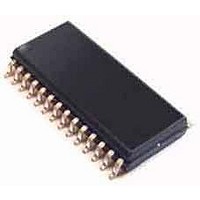
NCV7608DWR2G ON Semiconductor, NCV7608DWR2G Datasheet - Page 5
NCV7608DWR2G
Manufacturer Part Number
NCV7608DWR2G
Description
8 CHANNEL DRIVER
Manufacturer
ON Semiconductor
Type
Configurable Low/High Side Driverr
Series
-r
Datasheet
1.NCV7608DWR2G.pdf
(23 pages)
Specifications of NCV7608DWR2G
Product
Driver ICs - Various
Rise Time
12 us
Fall Time
12 us
Supply Voltage (max)
34 V
Supply Voltage (min)
- 0.3 V
Supply Current
1 us
Maximum Operating Temperature
- 40 C
Mounting Style
SMD/SMT
Package / Case
SOIC-28
Minimum Operating Temperature
+ 150 C
Number Of Drivers
8
Output Current
350 mA
Output Voltage
34 V to 48 V
Input Type
SPI
Number Of Outputs
8
On-state Resistance
1.2 Ohm
Current - Output / Channel
-
Current - Peak Output
350mA
Voltage - Supply
3.15 V ~ 5.25, 5.5 V ~ 28 V
Operating Temperature
-
Mounting Type
Surface Mount
Lead Free Status / Rohs Status
Lead free / RoHS Compliant
Available stocks
Company
Part Number
Manufacturer
Quantity
Price
Company:

Part Number:
NCV7608DWR2G
Manufacturer:
ON Semiconductor
Quantity:
317
Part Number:
NCV7608DWR2G
Manufacturer:
ON/安森美
Quantity:
20 000


Stresses exceeding Maximum Ratings may damage the device. Maximum Ratings are stress ratings only. Functional operation above the
Recommended Operating Conditions is not implied. Extended exposure to stresses above the Recommended Operating Conditions may affect
device reliability.
1. In this configuration lower voltage limit is due to drain−gate clamp.
2. Internally limited.
3. 1638000 pulses (triangular), 350 mA peak, VS = 18 V, 47 W, 410 mH, T
4. 1 oz copper, 300 mm
MAXIMUM RATINGS
RECOMMENDED OPERATING CONDITIONS
THERMAL CONDITIONS
Digital supply input voltage (V
Battery supply input voltage (VS)
Digital I/O pin voltage (IN5, IN6, IN7, IN8, SI, SO, CSB, SCLK, EN)
Configured for High−Side Operation
Configured for Low−Side Operation
Clamping energy
Electrostatic Discharge (VS, D1−D8, S1−S8)
Electrostatic Discharge (All Other Pins)
AECQ10x−12−REVA
SHORT−CIRCUIT
RELIABILITY CHARACTERIZATION
Moisture Sensitivity Level
Digital supply input voltage (V
Battery supply input voltage (VS)
DC Output current (Sx,Dx)
Junction temperature
Junction−to−Lead (Y
Junction−to−Ambient (R
DC input supply voltage
Transient input supply voltage
Drain = VS
Source Output DC Voltage (S1−S8)
Transient Source Output voltage (S1−S8)
Source = GND
Drain Output DC Voltage (D1−D8)
Transient Drain Output Voltage (D1−D8)
Maximum (single pulse)
Repetitive (multiple pulse) (Note )3
Human Body Model (100 pF, 1.5 kW)
Machine Model (200 pF)
Charged Device
Human Body Model (100 pF, 1.5 kW)
Machine Model (200pF)
Charged Device
JL
2
, Y
qJA
copper area, 0.062″ thick FR4.
(Voltages are with respect to device substrate)
JL
, q
)
JA
CC
CC
) (Note 4)
)
)
Rating
Rating
Thermal Parameters
http://onsemi.com
5
A
= 85°C.
VSHSXDCmax
VSHSXACmax
VDLSXDCmax
VDLSXACmax
VSDCmax
VSACmax
VCCmax
Symbol
VIOmax
Symbol
VCCop
AECsc
Wmax
ESD4
ESD2
Wrep
Vsop
MSL
Ixop
T
J
3.15
Min
Min
−40
−1 to 34 (Note 1)
−1 to 48 (Note 2)
5.5
25
−
−4000 to 4000
−1000 to 1000
−2000 to 2000
−1000 to 1000
−
−200 to 200
−200 to 200
−0.3 to 34
−0.3 to 40
−29 to 34
−0.3 to 7
−0.3 to 7
Grade B
−1 to 34
Value
MSL3
Value
100
20
Max
5.25
Max
350
150
28
40
82
°C/W
°C/W
Unit
Unit
Unit
mA
mJ
mJ
°C
V
V
V
V
V
V
V
V
V
V
V
V
−
Related parts for NCV7608DWR2G
Image
Part Number
Description
Manufacturer
Datasheet
Request
R

Part Number:
Description:
Ncv7608 Octal Configurable Low/high Side Driver
Manufacturer:
ON Semiconductor
Datasheet:
Part Number:
Description:
ON Semiconductor [VOLTAGE REGULATOR]
Manufacturer:
ON Semiconductor
Datasheet:
Part Number:
Description:
357-036-542-201 CARDEDGE 36POS DL .156 BLK LOPRO
Manufacturer:
ON Semiconductor
Datasheet:
Part Number:
Description:
357-036-542-201 CARDEDGE 36POS DL .156 BLK LOPRO
Manufacturer:
ON Semiconductor
Datasheet:
Part Number:
Description:
357-036-542-201 CARDEDGE 36POS DL .156 BLK LOPRO
Manufacturer:
ON Semiconductor
Datasheet:
Part Number:
Description:
357-036-542-201 CARDEDGE 36POS DL .156 BLK LOPRO
Manufacturer:
ON Semiconductor
Datasheet:
Part Number:
Description:
357-036-542-201 CARDEDGE 36POS DL .156 BLK LOPRO
Manufacturer:
ON Semiconductor
Datasheet:
Part Number:
Description:
357-036-542-201 CARDEDGE 36POS DL .156 BLK LOPRO
Manufacturer:
ON Semiconductor
Datasheet:
Part Number:
Description:
357-036-542-201 CARDEDGE 36POS DL .156 BLK LOPRO
Manufacturer:
ON Semiconductor
Datasheet:
Part Number:
Description:
357-036-542-201 CARDEDGE 36POS DL .156 BLK LOPRO
Manufacturer:
ON Semiconductor
Datasheet:
Part Number:
Description:
357-036-542-201 CARDEDGE 36POS DL .156 BLK LOPRO
Manufacturer:
ON Semiconductor
Datasheet:
Part Number:
Description:
357-036-542-201 CARDEDGE 36POS DL .156 BLK LOPRO
Manufacturer:
ON Semiconductor
Datasheet:
Part Number:
Description:
Manufacturer:
ON Semiconductor
Datasheet:
Part Number:
Description:
Manufacturer:
ON Semiconductor
Datasheet: