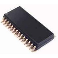
NCV7608DWR2G ON Semiconductor, NCV7608DWR2G Datasheet - Page 6

NCV7608DWR2G
Manufacturer Part Number
NCV7608DWR2G
Description
8 CHANNEL DRIVER
Manufacturer
ON Semiconductor
Type
Configurable Low/High Side Driverr
Series
-r
Datasheet
1.NCV7608DWR2G.pdf
(23 pages)
Specifications of NCV7608DWR2G
Product
Driver ICs - Various
Rise Time
12 us
Fall Time
12 us
Supply Voltage (max)
34 V
Supply Voltage (min)
- 0.3 V
Supply Current
1 us
Maximum Operating Temperature
- 40 C
Mounting Style
SMD/SMT
Package / Case
SOIC-28
Minimum Operating Temperature
+ 150 C
Number Of Drivers
8
Output Current
350 mA
Output Voltage
34 V to 48 V
Input Type
SPI
Number Of Outputs
8
On-state Resistance
1.2 Ohm
Current - Output / Channel
-
Current - Peak Output
350mA
Voltage - Supply
3.15 V ~ 5.25, 5.5 V ~ 28 V
Operating Temperature
-
Mounting Type
Surface Mount
Lead Free Status / Rohs Status
Lead free / RoHS Compliant
Available stocks
Company
Part Number
Manufacturer
Quantity
Price
Company:
Part Number:
NCV7608DWR2G
Manufacturer:
ON Semiconductor
Quantity:
317
Part Number:
NCV7608DWR2G
Manufacturer:
ON/安森美
Quantity:
20 000
ELECTRICAL CHARACTERISTICS
specified)
GENERAL PARAMETERS
THERMAL RESPONSE
POWER OUTPUTS, DC CHARACTERISTICS
5. Refer to Figures 12 and 17 for the VS standby current behavior.
6. Refer to Figure 10. I(VS) versus Temperature.
7. Refer to Figure 16 for the V
8. Refer to Figures 11 and 14 for R
9. Refer to Figure 15 for output leakage current behavior.
10. Refer to Figures 18 and 19 for open load diagnostic current behavior.
11. Refer to Figure 13 for current limit behavior.
VS Supply Current
VCC Supply Current
VCC Power−on reset Threshold
VCC Power−on reset Hysteresis
VS Undervoltage Threshold
VS Undervoltage Hysteresis
VS Overvoltage Threshold
VS Overvoltage Hysteresis
Thermal Warning
Thermal Warning Hysteresis
Overtemperature Shutdown
Overtemperature Shutdown
hysteresis
Ratio of Overtemperature
Shutdown to Thermal Warning
Output Transistor R
(Note 8)
Output Leakage Current (Note 9)
Open Load Diagnostic Sink
Current Low Side
Open Load Diagnostic Source
Current High Side (Note 10)
Open load detection threshold
voltage, VD (LS)
Open load detection threshold
voltage, VS (HS)
Over Current (Note 11)
Output fault filter time
Characteristic
Standby (Note 5)
Run (Note 6)
Standby (Note 7)
Run
High−Side
Low−Side
Over Current
Open Load
DS(on)
CC
standby current behavior.
DS(on)
RonVSminx
VCCPOR
TSTOTW
IdiagHSx
RonOPx
IdiagLSx
Symbol
VCChys
VSUhys
VSOhys
TLIMHY
RonVS3
IQVS85
IVCCop
IQVCC
VOLDx
VOLSx
IlimHS
VSUV
VSOV
IlimLS
TFOC
IVSop
TFOL
TWH
TLIM
(−40°C < T
Ilkgx
behavior.
TW
J
< 150°C, 5.5 V < VS < 28 V, 3.15 V < V
En = 0 V, 0 V v V
= 13.2 V, Sx = 0 V, −40°C < T
All channels Active
EN = 0 V, CSB = V
all channels active, I
VS increasing
Not ATE tested
Not ATE tested
Not ATE tested
Not ATE tested
Not ATE tested
VS = 8 V, I(Dx) = 200 mA
VS = 5.5 V, I(Dx) = 200 mA
VS = 3 V, I(Dx) = 200 mA
VS = Dx = 16 V, Sx = 0 V
Dx = 2.6 V, Sx = 0 V, Output disabled
Dx = VS, Sx = VS − 2.6 V, Output
disabled
−40°C < T
VS = 16 V
VS = 16 V
V
VS increasing
CC
http://onsemi.com
increasing
J
< 125°C
6
Conditions
CC
CC
(SO)
v 5.25 V, Dx = VS
, −40°C < T
= 0
J
< 85°C
J
< 85°C
CC
< 5.25 V, EN = V
−1.90
VS−3
−500
1.05
0.80
Min
100
100
120
155
100
2.6
2.5
1.0
1.0
32
50
50
0
−
0
−
−
−
−
−
−
−
−1.35
−330
1.20
1.35
Typ
200
200
145
175
215
VS−
100
100
2.8
2.5
1.2
1.4
1.6
2.8
36
30
30
2.0
1
−
1
−
−
2
CC
, unless otherwise
−0.80
VS−1
−150
Max
1.90
170
195
350
200
200
3.0
3.0
4.0
2.8
5.6
9.9
3.0
12
40
5
5
3
−
−
−
−
5
−
°C/°C
Unit
mA
mA
mV
mV
mA
mA
mA
mA
mA
°C
°C
°C
°C
ms
W
V
V
V
V
V
V
A


