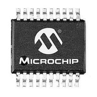
PIC16F1507-I/SO Microchip Technology, PIC16F1507-I/SO Datasheet - Page 13

PIC16F1507-I/SO
Manufacturer Part Number
PIC16F1507-I/SO
Description
3.5KB Flash, 128B RAM, 18 I/O, CLC, CWG, DDS, 10-bit ADC 20 SOIC .300in TUBE
Manufacturer
Microchip Technology
Series
PIC® 16Fr
Datasheets
1.PIC16F1507-EML.pdf
(266 pages)
2.PIC16F1507-EML.pdf
(26 pages)
3.PIC16F1507-EML.pdf
(40 pages)
Specifications of PIC16F1507-I/SO
Processor Series
PIC16
Core
PIC16F
Data Bus Width
8 bit
Program Memory Type
Flash
Program Memory Size
3.5 KB
Data Ram Size
128 B
Interface Type
ICSP
Maximum Clock Frequency
20 MHz
Number Of Programmable I/os
18
Number Of Timers
3
Operating Supply Voltage
2.3 V to 5.5 V
Maximum Operating Temperature
+ 85 C
Mounting Style
SMD/SMT
Package / Case
SOIC-20
Minimum Operating Temperature
- 40 C
Operating Temperature Range
- 40 C to + 85 C
Supply Current (max)
30 uA
Core Processor
PIC
Core Size
8-Bit
Speed
20MHz
Connectivity
-
Peripherals
Brown-out Detect/Reset, POR, PWM, WDT
Number Of I /o
17
Eeprom Size
-
Ram Size
128 x 8
Voltage - Supply (vcc/vdd)
2.3 V ~ 5.5 V
Data Converters
A/D 12x10b
Oscillator Type
Internal
Operating Temperature
-40°C ~ 85°C
Lead Free Status / Rohs Status
Details
Available stocks
Company
Part Number
Manufacturer
Quantity
Price
Part Number:
PIC16F1507-I/SO
Manufacturer:
MICROCHI
Quantity:
20 000
2011 Microchip Technology Inc.
FIGURE 1-4:
1.5.4
Once the data inputs are selected, they can be mapped into each of the four gates. The
output of each gate will differ according to the logic function selected. To select an input
into a gate, simply hover over the desired “X” and click once. The cursor arrow will have
changed to the pointer and a line extending the input into the gate will appear. To invert
the signal, click again where the “X” was and now a bubble should appear, indicating
an inversion. If clicked once more, the bubble and line should disappear and default
back to the original unconnected state.
1.5.5
Each of the gate outputs can be inverted. To do so, simply click once on the output of
an individual gate for a bubble to appear. The output is now inverted. To undo this, click
the bubble again for it to disappear. It is important to note that any gate with no inputs
selected will have its output default to the Off state (logic zero). If a constant logic one
is desired then invert the default logic zero by clicking the output for the inverting bub-
ble. Figure 1-5 shows the setup of having F
to Gate 2 with its output inverted.
FIGURE 1-5:
Gate Inputs
Gate Outputs
SELECTION FOSC AS AN INPUT FOR TWO DIFFERENT
GATES
GATE INPUT/OUTPUT WITH INVERSION
OSC
and an inverted Timer0 OVF as inputs
DS41597A-page 13


