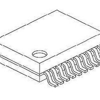
PIC16F1507-I/SS Microchip Technology, PIC16F1507-I/SS Datasheet - Page 15

PIC16F1507-I/SS
Manufacturer Part Number
PIC16F1507-I/SS
Description
3.5KB Flash, 128B RAM, 18 I/O, CLC, CWG, DDS, 10-bit ADC 20 SSOP .209in TUBE
Manufacturer
Microchip Technology
Series
PIC® 16Fr
Datasheets
1.PIC16F1507-EML.pdf
(266 pages)
2.PIC16F1507-EML.pdf
(26 pages)
3.PIC16F1507-EML.pdf
(40 pages)
Specifications of PIC16F1507-I/SS
Processor Series
PIC16
Core
PIC16F
Data Bus Width
8 bit
Program Memory Type
Flash
Program Memory Size
3.5 KB
Data Ram Size
128 B
Interface Type
ICSP
Maximum Clock Frequency
20 MHz
Number Of Programmable I/os
18
Number Of Timers
3
Operating Supply Voltage
2.3 V to 5.5 V
Maximum Operating Temperature
+ 85 C
Mounting Style
SMD/SMT
Package / Case
SSOP-20
Minimum Operating Temperature
- 40 C
Operating Temperature Range
- 40 C to + 85 C
Supply Current (max)
30 uA
Core Processor
PIC
Core Size
8-Bit
Speed
20MHz
Connectivity
-
Peripherals
Brown-out Detect/Reset, POR, PWM, WDT
Number Of I /o
17
Eeprom Size
-
Ram Size
128 x 8
Voltage - Supply (vcc/vdd)
2.3 V ~ 5.5 V
Data Converters
A/D 12x10b
Oscillator Type
Internal
Operating Temperature
-40°C ~ 85°C
Lead Free Status / Rohs Status
Details
Available stocks
Company
Part Number
Manufacturer
Quantity
Price
Company:
Part Number:
PIC16F1507-I/SS
Manufacturer:
MICROCHIP
Quantity:
5 000
Part Number:
PIC16F1507-I/SS
Manufacturer:
MICROCHIP/微芯
Quantity:
20 000
1.6
2011 Microchip Technology Inc.
SAVING/LOADING
1.5.7
The output from the logic block is fed to the last stage of the CLC, the inversion gate.
To invert the output, click on the buffer output pin once for a bubble to appear. From
here, the output can be routed to other peripherals, an output pin, or back to the CLC
input. An interrupt can be enabled upon a rising and/or falling edge from the CLC
output.
Figure 1-7 shows the configuration for enabling the module, enabling the output to the
CLCx output pin, and producing an interrupt upon a rising edge being detected. The
CLC output will also be inverted.
FIGURE 1-7:
The program provides convenient methods in saving or loading the design. When the
design is concluded and ready to be implemented in software, click the File pull-down
menu in the top-left corner of the dialog box as shown in Figure 1-8.
FIGURE 1-8:
Then click file>Save ASSY code or Save C code, depending on the desired output
language. The code for all configured CLCs of the selected device will be included in
the output file. The resultant file will have an .inc extension. Figure 1-7 shows
example output code for the setup as seen in Figure 1-6, with the inclusion of the
AND-OR logic block and the rest having default settings. The device used in the
example is a PIC16F1507 with module CLC1.
Output Control
CLC OUTPUT OPTIONS
LOCATION OF LOADING AND SAVING CODE IN THE
PROGRAM
DS41597A-page 15


