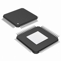
PIC24FJ256DA210T-I/BG Microchip Technology, PIC24FJ256DA210T-I/BG Datasheet - Page 3

PIC24FJ256DA210T-I/BG
Manufacturer Part Number
PIC24FJ256DA210T-I/BG
Description
16-bit, 256KB Flash, 96K RAM, USB, Graphics 121 XBGA 10x10x1.20mm T/R
Manufacturer
Microchip Technology
Series
PIC® 24Fr
Specifications of PIC24FJ256DA210T-I/BG
Core Processor
PIC
Core Size
16-Bit
Speed
32MHz
Connectivity
I²C, IrDA, SPI, UART/USART, USB OTG
Peripherals
Brown-out Detect/Reset, GFX, LVD, POR, PWM, WDT
Number Of I /o
84
Program Memory Size
256KB (85.5K x 24)
Program Memory Type
FLASH
Ram Size
96K x 8
Voltage - Supply (vcc/vdd)
2.2 V ~ 3.6 V
Data Converters
A/D 24x10b
Oscillator Type
Internal
Operating Temperature
-40°C ~ 85°C
Package / Case
121-TFBGA
Lead Free Status / RoHS Status
Lead free / RoHS Compliant
Eeprom Size
-
Lead Free Status / RoHS Status
Lead free / RoHS Compliant
Available stocks
Company
Part Number
Manufacturer
Quantity
Price
Company:
Part Number:
PIC24FJ256DA210T-I/BG
Manufacturer:
Microchip Technology
Quantity:
10 000
Silicon Errata Issues
1. Module: Oscillator (Two-Speed Start-up)
2. Module: Resets
3. Module: Enhanced PMP
2011 Microchip Technology Inc.
Note:
Two-Speed Start-up is not functional. Leaving
the IESO Configuration bit in its default state
(Two-Speed Start-up enabled) may result in
unpredictable operation.
Work around
None. Always program the IESO Configuration
bit to disable the feature (CW2<15> = 0).
Affected Silicon Revisions
On Brown-out Resets and External (Master Clear)
Resets, the POR bit may also become set. This
may cause Brown-out and External Reset condi-
tions to be indistinguishable from a Power-on
Reset.
Work around
None.
Affected Silicon Revisions
The module is not write-compatible with slave
devices that require data to be present before the
Write strobe is asserted. The module has no con-
figuration provision to output data before asserting
the Write strobe.
Since most slave devices require valid input data
to be present before the Write strobe is de-
asserted, the significance of this issue is thought to
be limited.
Work around
None.
Affected Silicon Revisions
A3
A3
A3
X
X
X
This document summarizes all silicon
errata issues from all revisions of silicon,
previous as well as current. Only the
issues indicated by the shaded column in
the following tables apply to the current
silicon revision (A3).
PIC24FJ256DA210 FAMILY
4. Module: A/D Converter
5. Module: Interrupts (INTx)
Once
(AD1CON1<15> = 1), it may continue to draw
extra current even if the module later is disabled
(AD1CON1<15> = 0).
Work around
In addition to disabling the module through the
ADON bit, set the corresponding PMD bit,
ADC1MD (PMD1<0>), to power it down completely.
Affected Silicon Revisions
Writing to the INTCON2 register may cause an
external interrupt event (inputs on INT0 through
INT4) to be missed. This only happens when the
interrupt event and the write event occur during
the same clock cycle.
Work around
If this cannot be avoided, write the data intended
for INTCON2 to any other register in the inter-
rupt block of the SFR (addresses, 0080h to
00E0h); then write the data to INTCON2.
Be certain to write the data to a register not
being actively used by the application, or to any
of the interrupt flag registers, in order to avoid
spurious interrupts. For example, if the inter-
rupts controlled by IEC5 are not being used in
the application, the code sequence would be:
IEC5 = 0x1E;
INTCON2 = 0x1E;
IEC5 = 0;
It is the user’s responsibility to determine an
appropriate
application.
Affected Silicon Revisions
A3
A3
X
X
the
register
A/D
module
for
the
DS80505C-page 3
is
particular
enabled


