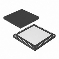
PIC32MX320F064HT-40I/MR Microchip Technology, PIC32MX320F064HT-40I/MR Datasheet - Page 4

PIC32MX320F064HT-40I/MR
Manufacturer Part Number
PIC32MX320F064HT-40I/MR
Description
64 KB Flash, 16 KB RAM, 40 MHz, 10-Bit ADC 64 QFN 9x9x0.9mm T/R
Manufacturer
Microchip Technology
Series
PIC® 32MXr
Datasheets
1.MA320002.pdf
(208 pages)
2.PIC32MX320F032H-40IPT.pdf
(48 pages)
3.PIC32MX320F032H-40IPT.pdf
(66 pages)
4.PIC32MX320F032H-40IPT.pdf
(22 pages)
Specifications of PIC32MX320F064HT-40I/MR
Core Processor
MIPS32® M4K™
Core Size
32-Bit
Speed
40MHz
Connectivity
I²C, IrDA, LIN, PMP, SPI, UART/USART
Peripherals
Brown-out Detect/Reset, POR, PWM, WDT
Number Of I /o
53
Program Memory Size
64KB (64K x 8)
Program Memory Type
FLASH
Ram Size
16K x 8
Voltage - Supply (vcc/vdd)
2.3 V ~ 3.6 V
Data Converters
A/D 16x10b
Oscillator Type
Internal
Operating Temperature
-40°C ~ 85°C
Package / Case
64-VFQFN, Exposed Pad
Processor Series
PIC32MX3xx
Core
MIPS
Data Bus Width
32 bit
Data Ram Size
16 KB
Interface Type
EUART, I2C, SPI
Maximum Clock Frequency
40 MHz
Number Of Programmable I/os
53
Number Of Timers
5
Maximum Operating Temperature
+ 85 C
Mounting Style
SMD/SMT
3rd Party Development Tools
52713-733, 52714-737
Development Tools By Supplier
PG164130, DV164035, DV244005, DV164005, DM320001, DM320002, MA320001
Minimum Operating Temperature
- 40 C
On-chip Adc
10 bit, 16 Channel
Lead Free Status / RoHS Status
Lead free / RoHS Compliant
Eeprom Size
-
Lead Free Status / Rohs Status
Details
PIC32MX
4.0
The PIC32MX family provides two possible physical
interfaces for connecting to and programming the
memory contents (Figure 4-1). For all programming
interfaces, the target device must be properly powered
and all required signals must be connected.
FIGURE 4-1:
4.1
One possible interface is the 4-wire JTAG (IEEE
1149.1) port. Table 4-1 lists the required pin connec-
tions. This interface uses the following four communi-
cation lines to transfer data to and from the PIC32MX
device being programmed:
• TCK – Test Clock Input
• TMS – Test Mode Select Input
• TDI – Test Data Input
• TDO – Test Data Output
TABLE 4-1:
DS61145G-page 4
MCLR
ENVREG
V
V
V
TDI
TDO
TCK
TMS
Legend: I = Input
Note 1:
DD
SS
DDCORE
Pin Name
Programmer
and AV
and AV
Device
CONNECTING TO THE DEVICE
4-Wire Interface
All power supply and ground pins must be connected, including analog supplies (AV
(AV
SS
DD
(1)
SS
(1)
).
4-WIRE INTERFACE PINS
MCLR
N/A
V
V
N/A
TDI
TDO
TCK
TMS
Programmer
+ MCLR, V
DD
SS
Pin Name
PROGRAMMING
INTERFACES
2-Wire
ICSP™
4-Wire
JTAG
OR
DD
, V
SS
O = Output
Pin Type
PIC32
O
P
P
P
P
I
I
I
I
Programming Enable
Enable for On-Chip Voltage Regulator
Power Supply
Ground
Regulated Power Supply for Core
Test Data In
Test Data Out
Test Clock
Test Mode State
These signals are described in the following four sec-
tions. Refer to the specific device data sheet for the
connection of the signals to the chip pins.
4.1.1
TCK is the clock that controls the updating of the TAP
controller and the shifting of data through the Instruc-
tion or selected Data register(s). TCK is independent of
the processor clock with respect to both frequency and
phase.
4.1.2
TMS is the control signal for the TAP controller. This
signal is sampled on the rising edge of TCK.
4.1.3
TDI is the test data input to the Instruction or selected
Data register(s). This signal is sampled on the rising
edge of TCK for some TAP controller states.
4.1.4
TDO is the test data output from the Instruction or Data
register(s). This signal changes on the falling edge of
TCK. TDO is only driven when data is shifted out,
otherwise the TDO is tri-stated.
P = Power
TEST CLOCK INPUT (TCK)
TEST MODE SELECT INPUT (TMS)
TEST DATA INPUT (TDI)
TEST DATA OUTPUT (TDO)
Pin Description
© 2010 Microchip Technology Inc.
DD
) and ground


