STK16C88-3WF35I Cypress Semiconductor Corp, STK16C88-3WF35I Datasheet - Page 3
STK16C88-3WF35I
Manufacturer Part Number
STK16C88-3WF35I
Description
STK16C88-3WF35I
Manufacturer
Cypress Semiconductor Corp
Datasheet
1.STK16C88-3WF35I.pdf
(15 pages)
Specifications of STK16C88-3WF35I
Format - Memory
RAM
Memory Type
NVSRAM (Non-Volatile SRAM)
Memory Size
256K (32K x 8)
Speed
35ns
Interface
Parallel
Voltage - Supply
4.5 V ~ 5.5 V
Operating Temperature
-40°C ~ 85°C
Package / Case
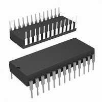
28-DIP (0.600", 15.24mm)
Lead Free Status / RoHS Status
Lead free / RoHS Compliant
Available stocks
Company
Part Number
Manufacturer
Quantity
Price
Company:

Part Number:
STK16C88-3WF35I
Manufacturer:
FREESCALE
Quantity:
101


Pin Configurations
Table 1. Pin Definitions - 28-Pin PDIP
Document Number: 001-50594 Rev. *A
Pin Name
DQ
A
0
V
V
WE
OE
CE
0
–A
SS
CC
-DQ
14
7
Alt
W
G
E
Power Supply Power Supply Inputs to the Device.
I/O Type
Input or
Ground
Output
Input
Input
Input
Input
Address Inputs. Used to select one of the 32,768 bytes of the nvSRAM.
Bidirectional Data I/O lines. Used as input or output lines depending on operation.
Write Enable Input, Active LOW. When the chip is enabled and WE is LOW, data on the
I/O pins is written to the specific address location.
Chip Enable Input, Active LOW. When LOW, selects the chip. When HIGH, deselects the
chip.
Output Enable, Active LOW. The active LOW OE input enables the data output buffers
during read cycles. Deasserting OE HIGH causes the I/O pins to tristate.
Ground for the Device. The device is connected to ground of the system.
Figure 1. Pin Diagram - 28-Pin PDIP
Description
STK16C88-3
Page 3 of 15
[+] Feedback
Related parts for STK16C88-3WF35I
Image
Part Number
Description
Manufacturer
Datasheet
Request
R

Part Number:
Description:
IC NVSRAM 256KBIT 45NS 28DIP
Manufacturer:
Cypress Semiconductor Corp
Datasheet:
Part Number:
Description:
STK16C88-WF25
Manufacturer:
Cypress Semiconductor Corp
Datasheet:
Part Number:
Description:
STK16C88-WF25I
Manufacturer:
Cypress Semiconductor Corp
Datasheet:
Part Number:
Description:
STK16C88-WF45I
Manufacturer:
Cypress Semiconductor Corp
Datasheet:

Part Number:
Description:
IC NVSRAM 256KBIT 35NS 28DIP
Manufacturer:
Cypress Semiconductor Corp
Datasheet:

Part Number:
Description:
Manufacturer:
Cypress Semiconductor Corp
Datasheet:
Part Number:
Description:
Manufacturer:
Cypress Semiconductor Corp
Datasheet:
Part Number:
Description:
Manufacturer:
Cypress Semiconductor Corp
Datasheet:
Part Number:
Description:
Manufacturer:
Cypress Semiconductor Corp
Datasheet:
Part Number:
Description:
Manufacturer:
Cypress Semiconductor Corp
Datasheet:
Part Number:
Description:
Manufacturer:
Cypress Semiconductor Corp
Datasheet:
Part Number:
Description:
Manufacturer:
Cypress Semiconductor Corp
Datasheet:
Part Number:
Description:
Manufacturer:
Cypress Semiconductor Corp
Datasheet: