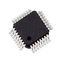
MC33910G5ACR2 Freescale, MC33910G5ACR2 Datasheet - Page 68

MC33910G5ACR2
Manufacturer Part Number
MC33910G5ACR2
Description
Manufacturer
Freescale
Datasheet
1.MC33910G5ACR2.pdf
(90 pages)
Specifications of MC33910G5ACR2
Turn Off Delay Time
10us
Number Of Drivers
2
Operating Temperature (min)
-40C
Operating Temperature (max)
125C
Operating Temperature Classification
Automotive
Lead Free Status / RoHS Status
Compliant
Available stocks
Company
Part Number
Manufacturer
Quantity
Price
Company:
Part Number:
MC33910G5ACR2
Manufacturer:
Freescale Semiconductor
Quantity:
10 000
ANALOG CIRCUITRY
operating conditions. A fully configurable window watchdog
circuit will reset the connected MCU in case of an overflow.
Two low power modes are available with several different
wake-up sources to reactivate the device. One analog / digital
input can be sensed or used as the wake-up source. The
device is capable of sensing the supply voltage (VSENSE)
and the internal chip temperature (CTEMP).
HIGH SIDE DRIVERS
with PWM capability are provided to drive small loads such as
Status LED’s or small lamps. Both Drivers can be configured
for periodic sense during low power modes.
MCU INTERFACE
through a standard 8-Bit SPI interface. Critical system events
such as Low- or High-voltage/Temperature conditions as well
Analog Integrated Circuit Device Data
Freescale Semiconductor
The 33910 is designed to operate under automotive
Two current and temperature protected High Side drivers
The 33910 is providing its control and status information
MC33910 - Functional Block Diagram
LIN Interface / Control
Integrated Supply
Analog Circuitry
MCU Interface and Output Control
SPI Interface
FUNCTIONAL INTERNAL BLOCK DESCRIPTION
Figure 35. Functional Internal Block Diagram
Integrated Supply
Analog Circuitry
Analog Output 0
Reset & IRQ Logic
HS - PWM Control
as over-current conditions in any of the driver stages can be
reported to the connected MCU via IRQ or RST. The High
Side driver outputs can be controlled via the SPI register as
well as the PWMIN input. The integrated LIN physical layer
interface can be configured via SPI register and its
communication is driven through the RXD and TXD device
pins. All internal analog sources are multiplexed to the
ADOUT0 pin.
VOLTAGE REGULATOR OUTPUTS
the 33910. The VDD main regulator output is designed to
supply a MCU with a precise 5.0 V. The switchable HVDD
output is dedicated to supply small peripherals as hall
sensors.
LIN PHYSICAL LAYER INTERFACE
layer interface with selectable slew rate and various
diagnostic features.
MCU Interface and Output Control
Drivers
Two independent voltage regulators are implemented on
The 33910 provides a LIN 2.0 compatible LIN physical
FUNCTIONAL INTERNAL BLOCK DESCRIPTION
High Side Drivers
LIN Physical Layer
HS1 - HS2
Interface
FUNCTIONAL DESCRIPTION
33910
68


