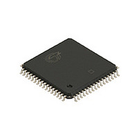
CY7C4225-15ASC Cypress Semiconductor Corp, CY7C4225-15ASC Datasheet - Page 8

CY7C4225-15ASC
Manufacturer Part Number
CY7C4225-15ASC
Description
Manufacturer
Cypress Semiconductor Corp
Datasheet
1.CY7C4225-15ASC.pdf
(22 pages)
Specifications of CY7C4225-15ASC
Configuration
Dual
Density
18Kb
Access Time (max)
10ns
Word Size
18b
Organization
1Kx18
Sync/async
Synchronous
Expandable
Yes
Bus Direction
Uni-Directional
Package Type
TQFP
Clock Freq (max)
66.7MHz
Operating Supply Voltage (typ)
5V
Operating Supply Voltage (min)
4.5V
Operating Supply Voltage (max)
5.5V
Supply Current
45mA
Operating Temp Range
0C to 70C
Operating Temperature Classification
Commercial
Mounting
Surface Mount
Pin Count
64
Lead Free Status / RoHS Status
Not Compliant
Maximum Ratings
(Above which the useful life may be impaired. For user guidelines,
not tested.)
Storage Temperature ....................................−65
Ambient Temperature with
Power Applied.................................................−55
Supply Voltage to Ground Potential .................−0.5V to +7.0V
DC Voltage Applied to Outputs
in High-Z State .....................................................−0.5V to +7.0V
Electrical Characteristics
Capacitance
Document Number: 001-45652 Rev. **
C
C
Parameter
V
V
V
V
I
I
I
I
I
I
Notes
IX
OS
OZL
CC
SB
OZH
4. T
5. See the last page of this specification for Group A subgroup testing information.
6. The Voltage on any input or I/O pin cannot exceed the power pin during power-up
7. The V
8. Test no more than one output at a time for not more than one second.
9. Input signals switch from 0V to 3V with a rise/fall time less than 3 ns, clocks and clock enables switch at 20 MHz, while the data inputs switch at 10 MHz. Outputs
10. All input signals are connected to V
11. Tested initially and after any design or process changes that may affect these parameters.
IN
OUT
OH
OL
IH
IL
[7]
[10]
[9]
[7]
or V
are unloaded.
[8]
A
is the “instant on” case temperature.
SS
Parameter
IH
.
and V
Output HIGH Voltage
Output LOW Voltage
Input HIGH Voltage
Input LOW Voltage
Input Leakage Current
Output Short Circuit
Current
Output OFF,
High Z Current
Operating Current
Standby Current
IL
[11]
specifications apply for all inputs except WXI, RXI. The WXI, RXI pin is not a TTL input. It is connected to either RXO, WXO of the previous device
Description
[6]
Input Capacitance
Output Capacitance
CC
Over the Operating Range
. All outputs are unloaded.
Description
V
I
V
I
V
V
V
OE > V
V
V
I
V
I
OH
OL
OUT
OUT
CC
CC
CC
CC
OUT
SS
CC
CC
Test Conditions
= 8.0 mA
= −2.0 mA
= Max.,
< V
= Max.
= Min.,
= Min.,
= Max.,
= Max.,
= 0 mA
= 0 mA
= GND
°
°
IH
C to +150
C to +125
O
,
< V
CC
Com’l
Ind’l
Com’l
Ind’l
°
°
C
C
T
V
[6]
A
CC
= 25
Min.
−3.0
−10
−90
−10
= 5.0V
2.4
2.2
°
DC Input Voltage ................................................. −3.0V to +7.0V
Output Current into Outputs (LOW)............................. 20 mA
Static Discharge Voltage ........................................... >2001V
(per MIL-STD-883, Method 3015)
Latch-up Current ..................................................... >200 mA
Operating Range
Test Conditions
-10
C, f = 1 MHz,
Commercial
Industrial
Max.
V
+10
+10
0.4
0.8
45
50
10
15
Range
CC
[4]
Min.
−3.0
−10
−90
−10
2.4
2.2
-15
Max.
Ambient Temperature
V
+10
+10
0.4
0.8
45
50
10
15
CC
-40
0
°
°
C to +70
Min.
C to +85
−3.0
−10
−90
−10
CY7C4425/4205/4215
CY7C4225/4235/4245
2.4
2.2
-25
Max.
Max.
5
7
V
+10
+10
°
0.4
0.8
45
50
10
15
C
°
CC
C
Min.
−3.0
−10
−90
−10
2.4
2.2
-35
5V ± 10%
5V ± 10%
Max.
V
+10
+10
V
0.4
0.8
Page 8 of 22
45
50
10
15
CC
Unit
CC
pF
pF
Unit
mA
mA
mA
mA
μA
μA
μA
V
V
V
V
[+] Feedback


