STK20C04WF35I Cypress Semiconductor Corp, STK20C04WF35I Datasheet
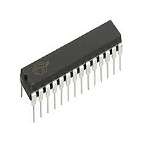
STK20C04WF35I

Manufacturer Part Number
STK20C04WF35I
Description
Manufacturer
Cypress Semiconductor Corp
Type
NVSRAMr
Datasheet

Specifications of STK20C04WF35I

Word Size
8b
Organization
512x8
Density
4Kb
Interface Type
Parallel
Access Time (max)
35ns
Operating Supply Voltage (typ)
5V
Package Type
PDIP
Operating Temperature Classification
Industrial
Operating Supply Voltage (max)
5.5V
Operating Supply Voltage (min)
4.5V
Operating Temp Range
-40C to 85C
Pin Count
28
Mounting
Through Hole
Supply Current
75mA
Lead Free Status / RoHS Status
Compliant
BLOCK DIAGRAM
FEATURES
• 25ns, 35ns and 45ns Access Times
• STORE to Nonvolatile Elements Initiated by
• RECALL to SRAM Initiated by Hardware or
• Automatic STORE Timing
• 10mA Typical I
• Unlimited READ, WRITE and RECALL Cycles
• 1,000,000 STORE Cycles to Nonvolatile Ele-
• 100-Year Data Retention over Full Industrial
• Commercial and Industrial Temperatures
DQ
DQ
DQ
DQ
DQ
DQ
DQ
DQ
March 2006
A
A
A
A
Hardware
Power Restore
ments
Temperature Range
5
6
7
8
0
1
2
3
4
5
6
7
CC
at 200ns Cycle Time
A
COLUMN DEC
STATIC RAM
COLUMN I/O
0
16 x 256
A
ARRAY
1
A
2
A
3
Obsolete - Not Recommend for new Designs
Quantum Trap
A
4
16 x 256
RECALL
STORE
1
DESCRIPTION
The Simtek STK20C04 is a fast static
volatile element incorporated in each static memory
cell. The
number of times, while independent nonvolatile data
resides in nonvolatile elements. Data may easily be
transferred from the
(the
ments to the
NE pin. Transfers from the Nonvolatile Elements to the
SRAM
matically on restoration of power. The STK20C04
combines the high performance and ease of use of a
fast
The STK20C04 features industry-standard pinout for
nonvolatile
Nonvolatile Static RAM
SRAM
QuantumTrap™ CMOS
STORE
Document Control # ML0001 rev 0.2
(the
CONTROL
RECALL
STORE/
SRAM
with nonvolatile data integrity.
RAM
RECALL
operation), or from the Nonvolatile Ele-
SRAM
G
NE
E
W
s in a 28-pin 600 mil plastic
can be read and written an unlimited
512 x 8 nvSRAM
(the
SRAM
operation) also take place auto-
PIN CONFIGURATIONS
PIN NAMES
DQ
DQ
DQ
V
NC
NE
A
A
A
A
A
A
A
A
SS
2
STK20C04
7
6
5
4
3
1
0
0
2
1
A
W
DQ
E
G
NE
V
V
RECALL
0
CC
SS
- A
1
2
3
4
5
6
7
8
9
10
11
12
13
14
0
to the Nonvolatile Elements
- DQ
8
7
28
27
26
25
24
23
22
21
20
19
18
17
16
15
operation), using the
DQ
DQ
V
A
NC
NC
G
NC
E
DQ
DQ
DQ
W
NC
Address Inputs
Write Enable
Data In/Out
Chip Enable
Output Enable
Nonvolatile Enable
Power (+ 5V)
Ground
CC
8
RAM
7
6
5
4
3
28 - 600 PDIP
with a non-
DIP
.

Related parts for STK20C04WF35I

STK20C04WF35I Summary of contents

Page 1

FEATURES • 25ns, 35ns and 45ns Access Times • STORE to Nonvolatile Elements Initiated by Hardware • RECALL to SRAM Initiated by Hardware or Power Restore • Automatic STORE Timing • 10mA Typical I at 200ns Cycle Time CC • ...

Page 2

STK20C04 ABSOLUTE MAXIMUM RATINGS Voltage on Input Relative to Ground . . . . . . . . . . . . . .–0.5V to 7.0V Voltage on Input Relative ...

Page 3

SRAM READ CYCLES #1 & #2 SYMBOLS NO. #1, #2 Alt Chip Enable Access Time ELQV ACS Read Cycle Time AVAV Address Access Time AVQV ...

Page 4

STK20C04 SRAM WRITE CYCLES #1 & #2 SYMBOLS NO Alt Write Cycle Time AVAV AVAV Write Pulse Width WLWH WLEH Chip Enable to End ...

Page 5

MODE SELECTION Note k: An automatic RECALL takes place at power up, starting when V STORE ...

Page 6

STK20C04 STORE INHIBIT/POWER-UP RECALL SYMBOLS NO. Standard 29 t Power-up RECALL Duration RESTORE 30 t STORE Cycle Duration STORE 31 V Low Voltage Trigger Level SWITCH 32 V Low Voltage Reset Level RESET Note o: t starts from the time ...

Page 7

RECALL CYCLES #1, #2 & #3 SYMBOLS NO NLQX ELQXR GLQXR NLNH ELNHR GLNH NLEL NLGL GLNL GLEL ...

Page 8

STK20C04 March 2006 8 Document Control # ML0001 rev 0.2 ...

Page 9

The STK20C04 has two modes of operation: mode and nonvolatile mode, determined by the state of the NE pin. When in SRAM ory operates as a standard fast static nonvolatile mode, data is transferred in parallel from to Nonvolatile Elements ...

Page 10

STK20C04 If the STK20C04 WRITE power-up , the data will be corrupted. RECALL SRAM To help avoid this situation, a 10K Ohm resistor should be connected either between W and system V or between E and system ...

Page 11

STK20C04 March 2006 ORDERING INFORMATION - Temperature Range Access Time Lead Finish Package 11 Document Control # ML0001 rev 0.2 STK20C04 Blank = Commercial (0 to 70° Industrial (–40 to 85° ...

Page 12

Document Revision History Date Revision December 2002 0.0 September 2003 0.1 February 2006 0.2 Summary Replaced 30 nsec device with 25 nsec device. Added lead-free lead finish Marked as Obsolete, Not recommended for new design. ...

Related keywords