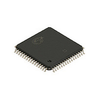
CY7C006A-20AI Cypress Semiconductor Corp, CY7C006A-20AI Datasheet - Page 9

CY7C006A-20AI
Manufacturer Part Number
CY7C006A-20AI
Description
Manufacturer
Cypress Semiconductor Corp
Datasheet
1.CY7C006A-20AI.pdf
(20 pages)
Specifications of CY7C006A-20AI
Density
128Kb
Access Time (max)
20ns
Sync/async
Asynchronous
Architecture
Not Required
Clock Freq (max)
Not RequiredMHz
Operating Supply Voltage (typ)
5V
Address Bus
14b
Package Type
TQFP
Operating Temp Range
-40C to 85C
Number Of Ports
2
Operating Supply Voltage (min)
4.5V
Operating Supply Voltage (max)
5.5V
Operating Temperature Classification
Industrial
Mounting
Surface Mount
Pin Count
64
Word Size
8b
Number Of Words
16K
Lead Free Status / RoHS Status
Not Compliant
Available stocks
Company
Part Number
Manufacturer
Quantity
Price
Company:
Part Number:
CY7C006A-20AI
Manufacturer:
CY
Quantity:
8
Company:
Part Number:
CY7C006A-20AI
Manufacturer:
CYPRESS
Quantity:
14
Document #: 38-06045 Rev. *D
Switching Characteristics
Data Retention Mode
The CY7C006A, CY7C007A, CY7C016A, and CY7C017A are
designed with battery backup in mind. Data retention voltage
and supply current are guaranteed over temperature. The
following rules ensure data retention:
Switching Waveforms
t
t
t
t
t
t
t
t
t
1. Chip Enable (CE) must be held HIGH during data retention,
2. CE must be kept between V
3. The RAM can begin operation >t
WB
WH
BDD
INS
INR
SOP
SWRD
SPS
SAA
INTERRUPT TIMING
SEMAPHORE TIMING
Read Cycle No. 1 (Either Port Address Access)
Notes:
DATA OUT
20. t
21. CE = V
22. R/W is HIGH for read cycles.
23. Device is continuously selected CE = V
24. OE = V
ADDRESS
within V
during the power-up and power-down transitions.
minimum operating voltage (4.5 volts).
Parameter
[20]
BDD
is a calculated parameter and is the greater of t
CC
IL
CC
.
, V
to V
in
= GND to V
PREVIOUS DATA VALID
R/W HIGH after BUSY (Slave)
R/W HIGH after BUSY HIGH (Slave)
BUSY HIGH to Data Valid
INT Set Time
INT Reset Time
SEM Flag Update Pulse (OE or SEM)
SEM Flag Write to Read Time
SEM Flag Contention Window
SEM Address Access Time
CC
– 0.2V.
[18]
CC
, T
A
t
= 25°C. This parameter is guaranteed but not tested.
OHA
CC
Description
– 0.2V and 70% of V
Over the Operating Range
IL
RC
. This waveform cannot be used for semaphore reads.
t
AA
after V
WDD
CC
–t
reaches the
PWE
[22, 23, 24]
(actual) or t
CC
t
RC
[12]
DDD
Min.
(continued)
10
11
0
5
5
–t
Timing
V
CE
ICC
SD
CC
–12
(actual).
Parameter
DR1
[1]
Max.
12
12
12
12
DATA VALID
Min.
13
10
CY7C006A
CY7C007A
CY7C016A
CY7C017A
0
5
5
4.5V
@ VCC
Data Retention Mode
Test Conditions
–15
V
CY7C006A/CY7C007A
CY7C016A/CY7C017A
CC
V
Max.
to V
CC
15
15
15
15
DR
> 2.0V
CC
= 2V
– 0.2V
t
OHA
Min.
15
10
0
5
5
[21]
4.5V
–20
Max.
20
20
20
20
Max.
1.5
Page 9 of 20
V
t
IH
RC
Unit
Unit
ns
ns
ns
ns
ns
ns
ns
ns
ns
mA
[+] Feedback


