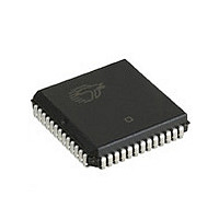
CY7C146-55JC Cypress Semiconductor Corp, CY7C146-55JC Datasheet - Page 8

CY7C146-55JC
Manufacturer Part Number
CY7C146-55JC
Description
Manufacturer
Cypress Semiconductor Corp
Datasheet
1.CY7C146-55JC.pdf
(15 pages)
Specifications of CY7C146-55JC
Density
16Kb
Access Time (max)
55ns
Sync/async
Asynchronous
Architecture
Not Required
Clock Freq (max)
Not RequiredMHz
Operating Supply Voltage (typ)
5V
Address Bus
22b
Package Type
PLCC
Operating Temp Range
0C to 70C
Number Of Ports
2
Supply Current
110mA
Operating Supply Voltage (min)
4.5V
Operating Supply Voltage (max)
5.5V
Operating Temperature Classification
Commercial
Mounting
Surface Mount
Pin Count
52
Word Size
8b
Number Of Words
2K
Lead Free Status / RoHS Status
Not Compliant
Available stocks
Company
Part Number
Manufacturer
Quantity
Price
Company:
Part Number:
CY7C146-55JC
Manufacturer:
CYPRESS
Quantity:
1 480
Company:
Part Number:
CY7C146-55JC
Manufacturer:
CY
Quantity:
3 588
Part Number:
CY7C146-55JC
Manufacturer:
CYPRESS/赛普拉斯
Quantity:
20 000
Company:
Part Number:
CY7C146-55JCT
Manufacturer:
CYPRESS
Quantity:
900
Switching Waveforms
Document #: 38-06031 Rev. *E
Note
20. If OE is LOW during a R/W controlled write cycle, the write pulse width must be the larger of t
ADDRESS
ADDRESS
ADDRESS
and for data to be placed on the bus for the required t
DATA
BUSY
DOUT
D
R/W
R/W
OUT
D
OE
CE
IN
INR
R
L
R
L
L
Figure 6. Read Cycle No. 3 (Read with BUSY Master: CY7C132 and CY7C136/CY7C136A)
Figure 7. Write Cycle No.1 (OE Three-States Data I/Os—Either Port)
t
HZOE
(continued)
t
SA
t
PS
SD
.
t
BLA
t
SCE
ADDRESS MATCH
t
AW
t
WC
t
RC
t
PWE
HIGH IMPEDANCE
ADDRESS MATCH
t
PWE
DATA VALID
t
SD
PWE
t
WDD
VALID
or t
CY7C136A, CY7C142, CY7C146
HZWE
+ t
t
SD
DDD
t
to allow the data I/O pins to enter high impedance
BHA
t
HD
t
HA
[12, 20]
CY7C132, CY7C136
t
BDD
VALID
Page 8 of 15
[+] Feedback


