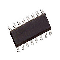
HCPL-788J Avago Technologies US Inc., HCPL-788J Datasheet - Page 19

HCPL-788J
Manufacturer Part Number
HCPL-788J
Description
OPTOCOUPLR AMP CURR SENSE 16SOIC
Manufacturer
Avago Technologies US Inc.
Series
-r
Type
Current Sensorr
Specifications of HCPL-788J
Package Type
SOIC
Operating Supply Voltage (typ)
5V
Voltage - Isolation
3750Vrms
Input Type
DC
Voltage - Supply
4.5 V ~ 5.5 V
Operating Temperature
-40°C ~ 85°C
Mounting Type
Surface Mount
Package / Case
16-SOIC (0.295", 7.50mm Width)
No. Of Amplifiers
1
Input Offset Voltage
3mV
Bandwidth
30kHz
Isolation Voltage
3.75kV
Supply Voltage Range
± 4.5V To ± 5.5V
Supply Current
20mA
Amplifier Case Style
SOIC
No. Of Pins
16
Rohs Compliant
No
Lead Free Status / RoHS Status
Not Compliant
Available stocks
Company
Part Number
Manufacturer
Quantity
Price
Company:
Part Number:
HCPL-788J
Manufacturer:
AVAGO
Quantity:
6 800
Part Number:
HCPL-788J
Manufacturer:
AVAGO/安华高
Quantity:
20 000
Company:
Part Number:
HCPL-788J#300E
Manufacturer:
AVAGO
Quantity:
15 000
Company:
Part Number:
HCPL-788J#500
Manufacturer:
AVAGO
Quantity:
25 000
Company:
Part Number:
HCPL-788J#500E
Manufacturer:
AVAGO
Quantity:
7 000
Company:
Part Number:
HCPL-788J-000E
Manufacturer:
AVAG0
Quantity:
12 000
Part Number:
HCPL-788J-500E
Manufacturer:
AVAGO/安华高
Quantity:
20 000
3. Isolation and Insulation
4. Accuracy
19
3.1: How many volts will the HCPL-788J
3.2: What happens if I don’t use the
4.1: What is the meaning of the offset
4.2: Can the signal to noise ratio be
4.3: I need 1% tolerance on gain. Does
4.4: The output doesn’t go all the way
4.5: Does the gain change if the internal
4.6: Why is gain defined as V
withstand?
470 pF output capacitors Avago
recommends?
errors and gain errors in terms of the
output?
improved?
Avago sell a more precise version?
to V
scale. Why not?
LED light output degrades with
time?
not V
on Figure 24?
REF
REF
when the input is above full
/512 mV as expected, based
REF
/504 mV,
The momentary (1 minute) withstand voltage is 5000 V rms per UL1577 and CSA
Component Acceptance Notice #5.
These capacitors are to reduce the narrow output spikes caused by high common
mode slew rates. If your application does not have rapid common mode voltage
changes, these capacitors are not needed.
For zero input, the output should ideally be
output relationship is V
voltage needed to make the output equal to
slope of the input/output relationship. For example, if V
7.937 V/V. For zero input, the output should be 2.000 V. Input offset voltage of ±3 mV
means the output voltage will be 2.000 V ±0.003*7.937 or 2.000 ±23.8 mV when the
input is zero. Gain tolerance of ±5% means that the slope will be 7.937 ±0.397. Over
the full range of ±3 mV input offset error and ±5% gain error, the output voltage will
be 2.000 ±25.0 mV when the input is zero.
Yes. Some noise energy exists beyond the 30 kHz bandwidth of the HCPL-788J.
An external RC low pass filter can be used to improve the signal to noise ratio. For
example, a 680 Ω, 4700 pF RC filter will cut the rms output noise roughly by a factor
of 2. This filter reduces the -3dB signal bandwidth only by about 10%. In applications
needing only a few kHz bandwidth even better noise performance can be obtained.
The noise spectral density is roughly 400 nV/
example, a 2 kHz (680 Ω, 0.1 μF) RC low pass filter reduces output noise to a typical
value of 0.08 mVrms.
At present Avago does not have a standard product with tighter gain tolerance. A 100
Ω variable resistor divider can be used to adjust the input voltage at pin 1, if needed.
Op-amps are used to drive V
swing nearly from rail to rail when there is no load current. The internal V
100 mV below the external V
sistors are not identical in capability. The net result is that the output can typically
swing to within 20 mV of GND
V
on maximum output voltage. The output remains linear and accurate for all inputs
between -200 mV and +200 mV. For the maximum possible swing range, separate V
and V
4.5 V or 4.096 V references for V
down to typically 20 mV).
No. The LED is used only to transmit a digital pattern. Gain is determined by a bandgap
voltage reference and the user-provided V
tion in the design of the product to ensure long life.
Ideally gain would be V
the average effective value of the internal 256 mV reference is 252 mV.
DD2
, the output cannot reach V
DD2
voltages can be used. Since 5.0 V is normally recommended for V
REF
REF
divided by 0.504 V. Offset errors change only the DC input
/512 mV, however, due to internal settling characteristics,
DD2
OUT
REF
REF
. In addition, the pullup and pulldown output tran-
2
allow the outputs to swing all the way up to V
(pin 12) and ABSVAL (pin 13). These op-amps can
exactly. This limitation has no effect on gain — only
and to within 150 mV of V
REF
1
. Avago has accounted for LED degrada-
/
—
2
Hz below 15 kHz (input referred). As an
1
of V
/
2
of V
REF
. The nominal slope of the input/
REF
. Gain errors change only the
REF
is 4.0 V, the gain should be
DD2
. When V
REF
DD2
DD2
is tied to
is about
, use of
REF
(and
REF


