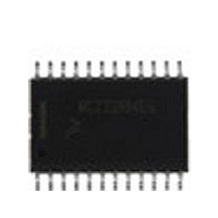
MCZ33291EGR2 Freescale, MCZ33291EGR2 Datasheet - Page 8

MCZ33291EGR2
Manufacturer Part Number
MCZ33291EGR2
Description
Manufacturer
Freescale
Datasheet
1.MCZ33291EGR2.pdf
(27 pages)
Specifications of MCZ33291EGR2
Switch Type
Low Side
Power Switch Family
MCZ33291
Input Voltage
-0.3 to 7V
Power Switch On Resistance
600mOhm
Output Current
500mA
Number Of Outputs
8
Mounting
Surface Mount
Supply Current
1mA
Package Type
SOIC W
Operating Temperature (min)
-40C
Operating Temperature Classification
Automotive
Pin Count
24
Power Dissipation
2W
Lead Free Status / RoHS Status
Compliant
Table 5. Dynamic Electrical Characteristics
Typical values noted reflect the approximate parameter mean at T
8
33291
ELECTRICAL CHARACTERISTICS
DYNAMIC ELECTRICAL CHARACTERISTICS
POWER OUTPUT TIMING
DIGITAL INTERFACE TIMING
Notes
Output Rise Time (V
Output Fall Time (V
Output Turn-ON Delay Time (V
Output Turn-OFF Delay Time (V
Output Short Fault Disable Report Delay
Output OFF Fault Report Delay
Required Low State Duration for
Falling Edge of
Falling Edge of SCLK to Rising Edge of
SI to Falling Edge of SCLK (Required for Setup Time)
Falling Edge of SCLK to SI (Required for Hold Time)
SO Rise Time (C
SO Fall Time (C
SI,
SI,
Time from Falling Edge of
Time from Rising Edge of
Time from Rising Edge of SCLK to SO Data Valid
0.2 V
28.
29.
30.
31.
32.
33.
34.
35.
36.
37.
Characteristics noted under conditions 4.5 V V
SFPD = 0.2 x V
SFPD = 0.2 x V
CS
CS
DD
, SCLK, Incoming Signal Rise Time
, SCLK, Incoming Signal Fall Time
Output Rise and Fall time respectively measured across a 26
Output Turn-ON Delay time measured from 50% rising edge of
Output Turn-OFF Delay time measured from 50% rising edge of
Propagation time of Short Fault Disable Report measured from 50% rising edge of
6.0 V and SFPD = 0.2 x V
Output OFF Fault Report Delay measured from 50% rising edge of
RST
Rise and Fall time of incoming SI,
Time required for output status data to be available for use at the SO pin.
Time required for output status data to be terminated at the SO pin.
Time required to obtain valid data out from SO following the rise of SCLK. See
SO
Low duration measured with outputs enabled and going to OFF or disabled condition.
CS
L
0.8 V
L
= 200 pF)
DD
DD
= 200 pF)
to Rising Edge of SCLK (Required Setup Time)
PWR
PWR
DD
, C
= 13 V, R
= 13 V, R
CS
CS
L
= 200 pF
to SO High Impedance
to SO Low Impedance
Characteristic
PWR
(32)
PWR
DD
RST
L
L
.
= 26 )
= 13 V, R
= 26 )
= 13 V, R
(V
CS
DYNAMIC ELECTRICAL CHARACTERISTICS
IL
CS
(31)
(34)
< 0.2 V
(34)
, and SCLK signals suggested for design consideration to prevent the occurrence of double pulsing.
(Required for Setup Time)
(28)
(28)
L
L
= 26
= 26 )
DD
(37)
)
(35)
(36)
(33)
)
DD
(29)
(30)
5.5 V, 9.0 V V
CS
CS
resistive load at 10% to 90% and 90% to 10% voltage points.
A
to 90% of Output OFF voltage (V
to 10% of Output OFF voltage (V
CS
= 25 C under nominal conditions, unless otherwise noted.
to 10% rising edge of Output OFF voltage (V
PWR
t
t
t
t
DLY (OFF)
DLY (OFF)
Symbol
t
SI (HOLD)
t
DLY (ON)
t
t
DLY (SF)
SO(DIS)
W(RST)
t
t
t
SO(EN)
t
t
SI (SU)
t
R (SO)
t
VALID
F (SO)
LEAD
t
R (SI)
F (SI)
LAG
t
t
16 V, -40 C T
R
F
Figure
CS
7, page 10.
to 10% Output OFF voltage (V
Min
0.4
0.4
1.0
1.0
Analog Integrated Circuit Device Data
70
70
–
–
–
–
–
–
–
–
–
–
–
–
A
PWR
125 C, unless otherwise noted.
PWR
) with R
) with R
Typ
150
150
5.0
5.0
15
15
50
50
50
25
25
25
25
65
–
–
–
–
Freescale Semiconductor
L
L
= 26
= 26
PWR
PWR
Max
250
250
167
167
167
110
110
105
20
20
50
50
83
83
50
50
50
50
resistive load.
).
resistive load.
), V
PWR
Unit
ns
ns
ns
ns
ns
ns
ns
ns
ns
ns
ns
ns
=
s
s
s
s
s
s


