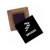
MPC8270CVVUPEA Freescale, MPC8270CVVUPEA Datasheet - Page 72

MPC8270CVVUPEA
Manufacturer Part Number
MPC8270CVVUPEA
Description
Manufacturer
Freescale
Datasheet
1.MPC8270CVVUPEA.pdf
(80 pages)
Specifications of MPC8270CVVUPEA
Family Name
MPC82XX
Device Core
PowerQUICC II
Device Core Size
32b
Frequency (max)
450MHz
Instruction Set Architecture
RISC
Operating Supply Voltage (max)
1.6V
Operating Supply Voltage (min)
1.45V
Operating Temp Range
-40C to 105C
Operating Temperature Classification
Industrial
Mounting
Surface Mount
Pin Count
480
Package Type
TBGA
Lead Free Status / RoHS Status
Compliant
Available stocks
Company
Part Number
Manufacturer
Quantity
Price
Company:
Part Number:
MPC8270CVVUPEA
Manufacturer:
Freescale Semiconductor
Quantity:
135
Company:
Part Number:
MPC8270CVVUPEA
Manufacturer:
FREE
Quantity:
4
Company:
Part Number:
MPC8270CVVUPEA
Manufacturer:
Freescale Semiconductor
Quantity:
10 000
Part Number:
MPC8270CVVUPEA
Manufacturer:
NXP/恩智浦
Quantity:
20 000
Package Description
9 Package Description
The following sections provide the package parameters and mechanical dimensions.
9.1 Package Parameters
Package parameters are provided in
72
1
2
3
4
5
6
7
Core Power
Ground
current, it is recommended to either pull unused pins to GND or VDDH, or to configure them as outputs.
signal on the MPC8275/MPC8270. New designs must connect B18 to GND and follow the suggestions in
Practices.” Old designs in which the MPC8275/MPC8270 is used as a drop-in replacement can leave the pin connected to
GND with the noise filtering capacitors.
external capacitor to operate the PLL. New designs should connect A18 (XFC) pin to GND. Old designs in which the
MPC8275/MPC8270 is used as a drop-in replacement can leave the pin connected to the current capacitor.
Should be tied to VDDH via a 2K Ω external pull-up resistor.
The default configuration of the CPM pins (PA[0–31], PB[4–31], PC[0–31], PD[4–31]) is input. To prevent excessive DC
Must be pulled down or left floating.
If PCI is not desired, must be pulled up or left floating.
Sphere is not connected to die.
GNDSYN (B18): This pin exists as a separate ground signal in MPC826x(A) devices; it does not exist as a separate ground
XFC (A18) pin: This pin is used in MPC826x(A) devices; it is not used in MPC8275/MPC8270 because there is no need for
MPC8275/MPC8270
Table 23. MPC8275 and MPC8270 (VR and ZQ Packages) Pinout List (continued)
MPC8280 PowerQUICC™ II Family Hardware Specifications, Rev. 1.8
Pin Name
Table
24.
MPC8275 only
L3, V4, W3, AC11, AD11, AB15,
U25, T24, J24, H25, F23, B19, D17,
C17, D10, C10
B18
C18, D4, D6, G2, L4, P1, R1, R4,
AC4, AE7, AC23, Y25, N24, J23,
A23, D23, D20, E18, A13, A16, K10,
K11, K12, K13, K14, K15, K16, K17,
L10, L11, L12, L13, L14, L15, L16,
L17, M10, M11, M12, M13, M14,
M15, M16, M17, N10, N11, N12,
N13, N14, N15, N16, N17, P10, P11,
P12, P13, P14, P15, P16, P17, R10,
R11,R12, R13, R14, R15, R16, R17,
T10, T11, T12, T13, T14, T15, T16,
T17, U10, U11, U12, U13, U14, U15,
U16, U17
6
, A18
7
Freescale Semiconductor
, A2, B1, B2, A5, C5,
Ball
Section 4.6, “Layout


