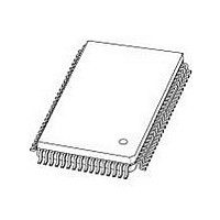
SAA7706H/N107 NXP Semiconductors, SAA7706H/N107 Datasheet - Page 30

SAA7706H/N107
Manufacturer Part Number
SAA7706H/N107
Description
Manufacturer
NXP Semiconductors
Datasheet
1.SAA7706HN107.pdf
(52 pages)
Specifications of SAA7706H/N107
Operating Temperature (min)
-40C
Operating Temperature (max)
85C
Operating Temperature Classification
Industrial
Mounting
Surface Mount
Lead Free Status / RoHS Status
Compliant
Available stocks
Company
Part Number
Manufacturer
Quantity
Price
Company:
Part Number:
SAA7706H/N107,518
Manufacturer:
NXP Semiconductors
Quantity:
10 000
Company:
Part Number:
SAA7706H/N107,557
Manufacturer:
NXP Semiconductors
Quantity:
10 000
Company:
Part Number:
SAA7706H/N107S,518
Manufacturer:
NXP Semiconductors
Quantity:
10 000
Company:
Part Number:
SAA7706H/N107S,557
Manufacturer:
NXP Semiconductors
Quantity:
10 000
Philips Semiconductors
8.16
Pin DSP_RESET is active LOW and requires an external
pull-up resistor. Between this pin and the V
capacitor should be connected to allow a proper switch-on
of the supply voltage. The capacitor value is such that the
chip is in reset as long as the power supply is not
stabilized. A more or less fixed relationship between the
DSP_RESET (pin) and the POM (pin) time constant is
mandatory.
The voltage on pin POM determines the current flowing in
the DACs. At 0 V on pin POM the DAC currents are zero
and so are the DAC output voltages.
At the V
(maximal) value. Long before the DAC outputs get to their
nominal output voltages, the DSP must be in working
mode to reset the output register: therefore the DSP time
constant must be shorter than the POM time constant. For
recommended capacitors see Figs 25 and 26.
The reset has the following function:
2001 Mar 05
handbook, full pagewidth
All I
The DSP status registers (DSP1 and DSP2) are reset
Car radio Digital Signal Processor (DSP)
2
C-bus bits are set to their default value
DSP reset
DDA2
RDS_CLOCK
RDS_DATA
voltage the DAC currents are at their nominal
block ready
Fig.19 Interface signals RDS decoder and microcontroller (buffer mode).
t w
start reading data
D0
T cy
SSD
ground a
D1
t HC
D2
t LC
30
When the level on pin DSP_RESET is at HIGH, the DSP
program (DSP1 and DSP2) starts to run.
8.17
Pins TSCAN, RTCB and SHTCB are used to put the chip
in test mode and to test the internal connections. Each pin
has an internal pull-down resistor to ground. In the
application these pins can be left open or connected to
ground.
The program counter of both DSPs are set to
address 0000H
The two output flags of DSP1 (DSP1_OUT1 and
DSP1_OUT2) are reset to logic 0. All the configurable
flags of DSP2 are reset to logic 0, however the four flags
available at the output of the chip are default configured
as input flags (DSP2_INOUT1, DSP2_INOUT2,
DSP2_INOUT3 and DSP2_INOUT4).
Test mode connections (pins TSCAN, RTCB
and SHTCB)
D13
D14
D15
Product specification
SAA7706H
MGU271


