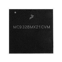
MC9328MX21CVM Freescale, MC9328MX21CVM Datasheet - Page 16

MC9328MX21CVM
Manufacturer Part Number
MC9328MX21CVM
Description
Manufacturer
Freescale
Datasheet
1.MC9328MX21CVM.pdf
(100 pages)
Specifications of MC9328MX21CVM
Operating Temperature (min)
-40C
Operating Temperature (max)
85C
Operating Temperature Classification
Industrial
Mounting
Surface Mount
Lead Free Status / RoHS Status
Compliant
Available stocks
Company
Part Number
Manufacturer
Quantity
Price
Company:
Part Number:
MC9328MX21CVM
Manufacturer:
Freescale Semiconductor
Quantity:
10 000
Company:
Part Number:
MC9328MX21CVMR2
Manufacturer:
Freescale Semiconductor
Quantity:
10 000
1. TA = 70
1. Data labeled Typical is not guaranteed, but is intended as an indication of the IC's potential performance.
2. For DSCR definition refer to the System Control chapter in the reference manual.
Specifications
Table 6
Table 7
3.4
The AC characteristics consist of output delays, input setup and hold times, and signal skew times. All
signals are specified relative to an appropriate edge of other signals. All timing specifications are specified
at a system operating frequency (HCLK) from 0 MHz to 133 MHz (core operating frequency 266 MHz)
with an operating supply voltage from V
16
ID
Input leakage current (no pull-up or pull-
down)
I/O leakage current
1
2 Sleep Current Standby current with Well Biasing System enabled.
Run Current
Parameter
shows the input and output capacitance for the device.
shows the power consumption for the device.
°
C for suffixes VK, VM, DVK, DVM, and SVK. TA = 85
AC Electrical Characteristics
Parameter
Input capacitance
Output capacitance
QVDD = QVDDX = 1.65 V, NVDD1 = 1.8 V.
NVDD2 through NVDD6 = VDDA = 3.1V.
Core = 266 MHz, System = 133 MHz.
MPEG4 Playback (QVGA) from MMC/SD card, 30fps,
44.1kHz audio.
Well Bias Control Register (WBCR) must be set as
follows:
WBCR:
CRM_WBS bits = 01
CRM_WBFA bit = 1
CRM_WBM bits = 001
CRM_SPA_SEL bit = 1
FMCR bit = 1
For WBCR definition refer to System Control Chapter
in the reference manual.
Parameter
Table 5. DC Characteristics (Continued)
Conditions
MC9328MX21 Technical Data, Rev. 3.4
Symbol
Table 6. Input/Output Capacitance
I
Table 7. Power Consumption
I
OZ
in
DD min
I/O = High impedance
Symbol
to V
V
Test Conditions
V
C
C
I/O
in
o
i
= 0 or NVDD
DD max
= NVDD or 0
state
°
C for suffixes CVK, CVM, and SCVK.
Min
under an operating temperature from T
–
–
I
QVDD = QVDDX = 1.65V, TA
QVDD = QVDDX = 1.65V, 25
QVDD = QVDDX = 1.55V, 25
NVDD2
Typ
–
–
through I
Min
I
QVDD
–
–
Symbol
I
NVDD1
I
STBY
+ I
Max
NVDD6
QVDDX
5
5
Typ
–
–
+ I
1
Freescale Semiconductor
VDDA
Units
pF
pF
°
°
1
Typ Max Units
120
320
Max
6.6
±1
±5
8
–
–
700
3.0
–
–
–
–
L
to T
Units
μA
μA
mA
mA
mA
mA
μA
μA
H
.


