HW-FMC-XM104-G Xilinx Inc, HW-FMC-XM104-G Datasheet
HW-FMC-XM104-G
Specifications of HW-FMC-XM104-G


Related parts for HW-FMC-XM104-G


HW-FMC-XM104-G Summary of contents
Page 1
FMC XM104 Connectivity Card User Guide UG536 (v1.1) September 24, 2010 ...
Page 2
Xilinx is disclosing this user guide, manual, release note, and/or specification (the "Documentation") to you solely for use in the development of designs to operate with Xilinx hardware devices. You may not reproduce, distribute, republish, download, display, post, or transmit ...
Page 3
Table of Contents Revision History Preface: About This Guide Guide Contents . . . . . . . . . . . . . . . . . . . . . . . . . . . . . ...
Page 4
FMC XM104 Connectivity Card User Guide UG536 (v1.1) September 24, 2010 ...
Page 5
... Guide Contents This manual contains the following chapter: • Chapter 1, Additional Documentation Prior to using the XM104, users should be familiar with Xilinx resources. See the following locations for additional documentation on Xilinx tools and solutions: • ISE® Design Suite: • Answer Browser: • ...
Page 6
Preface: About This Guide 6 www.xilinx.com FMC XM104 Connectivity Card User Guide UG536 (v1.1) September 24, 2010 ...
Page 7
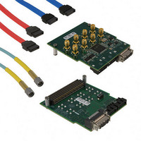
XM104 Overview This document describes the FPGA Mezzanine Card (FMC) XM104 connectivity module, referred to as the XM104 in this guide. A Description Quick Start System Requirements Hardware Table 1-1 details the board validated to support the XM104. The ML605 ...
Page 8
Chapter 1: XM104 Software Example designs that use this hardware are not provided at this time. Package Contents The following items are included in the XM104 shipment: • XM104 card • Four (4) mounting screws • Two (2) standoffs • ...
Page 9
X-Ref Target - Figure 1-1 Figure 1-1: Installation of XM104 to Board FMC HPC Connector Technical Support Xilinx offers technical support for this product only when used in conjunction with boards listed in Table technical support at www.xilinx.com/support. FMC XM104 ...
Page 10
Chapter 1: XM104 Board Technical Description The XM104 provides a number of connectors which break out the FPGA multi-gigabit transceiver (MGT) interface signals to and from the board interface. block diagram of the XM104. Each MGT data port interface consists ...
Page 11
Detailed Description The numbered features in page 12. For full functionality, the XM104 must be installed on a board FMC connector supporting high pin count interfaces. X-Ref Target - Figure 1-3 FMC XM104 Connectivity Card User Guide UG536 (v1.1) September ...
Page 12
Chapter 1: XM104 Table 1-2: XM104 Features Number Feature J1: Ten sets of FPGA multi-gigabit transceiver data port signals, a VITA 57.1 FMC HPC small number of FPGA single ended control signals from the board, 1 connector clocks and power. ...
Page 13
VITA 57.1 FMC HPC Connector J1 This connector interfaces to the board containing the Xilinx FPGA and mating FMC connector. The XM104 uses Samtec FMC HPC connector part number ASP-134488-01. The XM104 connector mates with an FMC connector. See ...
Page 14
Chapter 1: XM104 4. Multi-Gigabit Transceiver Data Port 2 - J11 SATA1 Board FPGA multi-gigabit transceiver Data Port 2 signals are wired to Serial ATA host connector J11 on the XM104. Data Port 2 connections between the XM104 FMC HPC ...
Page 15
Multi-Gigabit Transceiver Data Ports [4: 10GE Base-CX4 Connector Board FPGA multi-gigabit transceiver Data Ports 4 through 7 are wired to a 10GE Base- CX4 connector J2 on the XM104. The four data port connections between the XM104 ...
Page 16
Chapter 1: XM104 8. PCA9543 IIC Switch The board’s serial IIC bus is wired to an EEPROM and a two-channel NXP (formerly Philips Semiconductor) PCA9543 IIC bus switch on the XM104 (as shown in page 10). The IIC bus switch ...
Page 17
The two downstream IIC devices connected to the PCA9543 are at the following IIC addresses: • Si570 IIC address is at 0x5D • Si5368 IIC address is at 0x68 FMC XM104 Connectivity Card User Guide UG536 (v1.1) September 24, 2010 ...
Page 18
Chapter 1: XM104 9. Clocking Circuits Two programmable clock circuits are provided on the XM104: • Silicon Labs Si570 • Silicon Labs Si5368 A Silicon Labs Si570 serial IIC bus re-programmable clock source provides a low-jitter clock with a user-programmable ...
Page 19
Silicon Labs Si5368 A Silicon Labs Si5368 any-rate precision clock multiplier/jitter attenuator integrated circuit provides a wide range of clocking applications for the Xilinx board and XM104 combination. the XM104 FMC HPC connector. from the board to the inputs of ...
Page 20
Chapter 1: XM104 Table 1-13: Si5368 Clock I/O Connections to FMC HPC Connector J1 (Cont’d) FMC Connector J1 Signal Name Pin G10 LA03_N G9 LA03_P H8 LA02_N H7 LA02_P Notes: 1. These signals are either inputs or outputs to the ...