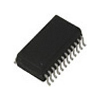
CAT5419WI-25-TE13 ON Semiconductor, CAT5419WI-25-TE13 Datasheet

CAT5419WI-25-TE13
Specifications of CAT5419WI-25-TE13
Related parts for CAT5419WI-25-TE13
CAT5419WI-25-TE13 Summary of contents
Page 1
Dual Digitally Programmable Potentiometers (DPP™) with 64 Taps and 2-wire Interface FEATURES Two linear-taper digital potentiometers 64 resistor taps per potentiometer End to end resistance 2.5 kΩ, 10 kΩ, 50kΩ or 100 kΩ Potentiometer control and memory access via 2 ...
Page 2
CAT5419 PIN DESCRIPTIONS SCL: Serial Clock The CAT5419 serial clock input pin is used to clock all data transfers into or out of the device. SDA: Serial Data The CAT5419 bidirectional serial data pin is used to transfer data into ...
Page 3
ABSOLUTE MAXIMUM RATINGS Parameters Temperature Under Bias Storage Temperature Range Voltage to any Pins with Respect with Respect to GND CC Package Power Dissipation Capability (T Lead Soldering Temperature (10 s) Wiper Current RECOMMENDED OPERATING CONDITIONS Parameters ...
Page 4
CAT5419 D.C. OPERATING CHARACTERISTICS Over recommended operating conditions unless otherwise stated. Symbol Parameter I Power Supply Current CC I Standby Current ( Input Leakage Current LI I Output Leakage Current LO V Input Low Voltage IL V ...
Page 5
WRITE CYCLES LIMITS Symbol Parameter t Write Cycle Time WR The write cycle is the time from a valid stop condition of a write sequence to the end of the internal program/erase cycle. During the write cycle, the bus interface ...
Page 6
CAT5419 SERIAL BUS PROTOCOL The following defines the features of the 2-wire bus protocol: (1) Data transfer may be initiated only when the bus is not busy. (2) During a data transfer, the data line must remain stable whenever the ...
Page 7
WRITE OPERATIONS In the Write mode, the Master device sends the START condition and the slave address information to the Slave device. After the Slave generates an acknowledge, the Master sends the instruction byte that defines the requested operation of ...
Page 8
CAT5419 INSTRUCTIONS AND REGISTER DESCRIPTION INSTRUCTIONS Slave Address Byte The first byte sent to the CAT5419 from the master/ processor is called the Slave/DPP Address Byte. The most significant four bits of the slave address are a device type identifier. ...
Page 9
WIPER CONTROL AND DATA REGISTERS Wiper Control Register (WCR) The CAT5419 contains two 6-bit Wiper Control Registers, one for each potentiometer. The Wiper Control Register output is decoded to select one of 64 switches along its resistor array. The contents ...
Page 10
CAT5419 The basic sequence of the three byte instructions is illustrated in Figure 8. These three-byte instructions exchange data between the WCR and one of the Data Registers. The WCR controls the position of the wiper. The response of the ...
Page 11
Figure 10. Increment/Decrement Timing Limits INC/DEC Command Issued SCL SDA R W INSTRUCTION FORMAT Read Wiper Control Register (WCR) S DEVICE ADDRESSES Write Wiper Control Register (WCR) S DEVICE ...
Page 12
CAT5419 INSTRUCTION FORMAT (continued) Global Transfer Data Register (DR) to Wiper Control Register (WCR) S DEVICE ADDRESSES Global Transfer Wiper Control Register (WCR) to Data Register (DR) S DEVICE ...
Page 13
PACKAGE OUTLINE DRAWINGS (1)(2) SOIC 24-Lead 300 mils ( PIN#1 IDENTIFICATION TOP VIEW D A SIDE VIEW Notes: (1) All dimensions in millimeters. Angles in degrees. (2) Complies with JEDEC MS-013. 2009 SCILLC. All rights reserved. Characteristics subject ...
Page 14
CAT5419 (1)(2) TSSOP 24-Lead 4.4 mm (Y) e TOP VIEW SIDE VIEW Notes: (1) All dimensions in millimeters. Angles in degrees. (2) Complies with JEDEC MO-153. Doc. No. MD-2115 Rev θ1 14 ...
Page 15
... CAT5419YI25 CAT5419YI10 CAT5419YI50 CAT5419YI00 Notes: (1) All packages are RoHS-compliant (Lead-free, Halogen-free). (2) This device used in the above example is a CAT5419WI-00-T1 (SOIC, Industrial Temperature, 100 kΩ, Tape & Reel). 2009 SCILLC. All rights reserved. Characteristics subject to change without notice (1) I Temperature Range I = Industrial (-40ºC to 85ºC) ...
Page 16
... Updated Package Outline Drawings Updated Example of Ordering Information Added MD- to document number 01-Dec-08 I Change logo and fine print to ON Semiconductor 31-Jul-09 J Update Ordering Information table ON Semiconductor and are registered trademarks of Semiconductor Components Industries, LLC (SCILLC). SCILLC reserves the right to make changes without further notice to any products herein ...


