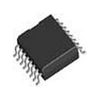
TP3054WM-X National Semiconductor, TP3054WM-X Datasheet

TP3054WM-X
Specifications of TP3054WM-X
Available stocks
Related parts for TP3054WM-X
TP3054WM-X Summary of contents
Page 1
... TTL or CMOS compatible digital interfaces n Maximizes line interface card circuit density n Dual-In-Line or PCC surface mount packages n See also AN-370, “Techniques for Designing with CODEC/Filter COMBO Circuits” 00867408 Order Number TP3054WM-X DS008674 March 2005 Dual-In-Line Package 00867401 Top View Order Number TP3054N-X ...
Page 2
Block Diagram Pin Descriptions Symbol Function V Negative power supply pin. BB ± −5V 5%. BB GNDA Analog ground. All signals are referenced to this pin Analog output of the receive power R amplifier. V Positive ...
Page 3
Pin Descriptions (Continued) Symbol Function MCLK Transmit master clock. Must be 1.536 X MHz, 1.544 MHz or 2.048 MHz. May be asynchronous with MCLK performance is realized from synchronous operation. FS Transmit frame sync pulse input which X enables BCLK ...
Page 4
Functional Description LONG FRAME SYNC OPERATION To use the long frame mode, both the frame sync pulses, FS and FS , must be three or more bit clock periods long with timing relationships specified in Figure 3. Based ...
Page 5
... Absolute Maximum Ratings If Military/Aerospace specified devices are required, please contact the National Semiconductor Sales Office/ Distributors for availability and specifications GNDA GNDA BB Voltage at any Analog Input or Output V Electrical Characteristics Unless otherwise noted, limits printed in BOLD characters are guaranteed for V −40˚C to +85˚C by correlation with 100% electrical testing at T production tests and/or product design and characterization ...
Page 6
Timing Specifications Unless otherwise noted, limits printed in BOLD characters are guaranteed for V −40˚C to +85˚C by correlation with 100% electrical testing at T production tests and/or product design and characterization. All signals referenced to GNDA. Typicals specified at ...
Page 7
7 www.national.com ...
Page 8
www.national.com 8 ...
Page 9
Transmission Characteristics Unless otherwise noted, limits printed in BOLD characters are guaranteed for V −40˚C to +85˚C by correlation with 100% electrical testing at T production tests and/or product design and characterization. GNDA = 0V 1.02 kHz, V ...
Page 10
Transmission Characteristics Unless otherwise noted, limits printed in BOLD characters are guaranteed for V −40˚C to +85˚C by correlation with 100% electrical testing at T production tests and/or product design and characterization. GNDA = 0V 1.02 kHz, V ...
Page 11
Transmission Characteristics Unless otherwise noted, limits printed in BOLD characters are guaranteed for V −40˚C to +85˚C by correlation with 100% electrical testing at T production tests and/or product design and characterization. GNDA = 0V 1.02 kHz, V ...
Page 12
Applications Information POWER SUPPLIES While the pins of the TP3050 family are well protected against electrical misuse recommended that the stan- dard CMOS practice be followed, ensuring that ground is connected to the device before any other connections ...
Page 13
Applications Information π-Pad Attenuator Note: See Application Note 370 for further details. dB 0.1 0.2 0.3 0.4 0.5 0.6 0.7 0.8 0.9 1 (Continued) TABLE 2. Attentuator Tables for Z1=Z2=300Ω (All ...
Page 14
Typical Synchronous Application www.national.com FIGURE 4. 14 00867406 ...
Page 15
... Physical Dimensions inches (millimeters) unless otherwise noted Dual-In-Line Package (M) Order Number TP3054WM-X NS Package Number M16B Molded Dual-In-Line Package (N) Order Number TP3054N-X NS Package Number N16E 15 www.national.com ...
Page 16
... BANNED SUBSTANCE COMPLIANCE National Semiconductor manufactures products and uses packing materials that meet the provisions of the Customer Products Stewardship Specification (CSP-9-111C2) and the Banned Substances and Materials of Interest Specification (CSP-9-111S2) and contain no ‘‘Banned Substances’’ as defined in CSP-9-111S2. ...


