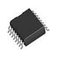
TP3054WM-X National Semiconductor, TP3054WM-X Datasheet - Page 2

TP3054WM-X
Manufacturer Part Number
TP3054WM-X
Description
Manufacturer
National Semiconductor
Type
PCMr
Datasheet
1.TP3054WM-X.pdf
(16 pages)
Specifications of TP3054WM-X
Number Of Channels
1
Number Of Adc's
1
Number Of Dac's
1
Package Type
SOIC W
Interface Type
Serial
Operating Supply Voltage (typ)
±5V
Number Of Adc Inputs
1
Number Of Dac Outputs
1
Operating Supply Voltage (max)
±5.25V
Operating Supply Voltage (min)
±4.75V
Pin Count
16
Mounting
Surface Mount
Lead Free Status / RoHS Status
Not Compliant
Available stocks
Company
Part Number
Manufacturer
Quantity
Price
Part Number:
TP3054WM-X
Manufacturer:
NS/国半
Quantity:
20 000
Part Number:
TP3054WM-X/NOPB
Manufacturer:
NS/国半
Quantity:
20 000
www.national.com
Block Diagram
Pin Descriptions
V
GNDA
VF
V
FS
D
BB
CC
R
R
R
Symbol
O
Negative power supply pin.
V
Analog ground. All signals are
referenced to this pin.
Analog output of the receive power
amplifier.
Positive power supply pin.
V
Receive frame sync pulse which
enables BCLK
D
Figure 2 and Figure 3 for timing details.
Receive data input. PCM data is shifted
into D
BB
CC
R
. FS
= −5V
= +5V
R
R
following the FS
is an 8 kHz pulse train. See
±
±
5%.
5%.
R
Function
to shift PCM data into
R
leading edge.
FIGURE 1.
2
BCLK
MCLK
Symbol
R
R
/CLKSEL The bit clock which shifts data into D
/PDN
after the FS
from 64 kHz to 2.048 MHz.
Alternatively, may be a logic input
which selects either 1.536 MHz/1.544
MHz or 2.048 MHz for master clock in
synchronous mode and BCLK
for both transmit and receive directions
(see Table 1).
Receive master clock. Must be 1.536
MHz, 1.544 MHz or 2.048 MHz. May be
asynchronous with MCLK
be synchronous with MCLK
performance. When MCLK
connected continuously low, MCLK
selected for all internal timing. When
MCLK
the device is powered down.
R
is connected continuously high,
R
leading edge. May vary
Function
00867402
X
, but should
R
X
is
for best
X
is used
X
R
is


