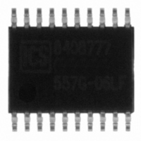
ICS557G-06LF IDT, Integrated Device Technology Inc, ICS557G-06LF Datasheet - Page 4

ICS557G-06LF
Manufacturer Part Number
ICS557G-06LF
Description
IC CLK BUFFER 1:4 HCSL 20-TSSOP
Manufacturer
IDT, Integrated Device Technology Inc
Type
Clock Bufferr
Datasheet
1.ICS557G-06LF.pdf
(11 pages)
Specifications of ICS557G-06LF
Input
HCSL, LVDS
Output
HCSL, LVDS
Frequency - Max
200MHz
Voltage - Supply
3.135 V ~ 3.465 V
Operating Temperature
0°C ~ 70°C
Mounting Type
Surface Mount
Package / Case
20-TSSOP
Frequency-max
200MHz
Number Of Clock Inputs
2
Mode Of Operation
Differential
Output Logic Level
HCSL/LVDS
Operating Supply Voltage (min)
3.135V
Operating Supply Voltage (typ)
3.3V
Operating Supply Voltage (max)
3.465V
Package Type
TSSOP
Operating Temp Range
0C to 70C
Operating Temperature Classification
Commercial
Signal Type
HCSL/LVDS
Mounting
Surface Mount
Pin Count
20
Lead Free Status / RoHS Status
Lead free / RoHS Compliant
Other names
557G-06LF
800-1064
800-1064-5
800-1064
800-1064
800-1064-5
800-1064
Available stocks
Company
Part Number
Manufacturer
Quantity
Price
Company:
Part Number:
ICS557G-06LF
Manufacturer:
IDT
Quantity:
2 006
Part Number:
ICS557G-06LFT
Manufacturer:
IDT
Quantity:
20 000
Output Structures
General PCB Layout Recommendations
For optimum device performance and lowest output phase
noise, the following guidelines should be observed.
1. Each 0.01µF decoupling capacitor should be mounted on
the component side of the board as close to the VDD pin as
possible.
2. No vias should be used between decoupling capacitor
and VDD pin.
3. The PCB trace to VDD pin should be kept as short as
possible, as should the PCB trace to the ground via.
Distance of the ferrite bead and bulk decoupling from the
device is less critical.
4. An optimum layout is one with all components on the
same side of the board, minimizing vias through other signal
layers (any ferrite beads and bulk decoupling capacitors can
be mounted on the back). Other signal traces should be
routed away from the ICS557-06.This includes signal traces
just underneath the device, or on layers adjacent to the
ground plane layer used by the device.
IDT® 2 TO 4 DIFFERENTIAL CLOCK MUX
ICS557-06
2 TO 4 DIFFERENTIAL CLOCK MUX
R
=2.3 mA
R
IREF
475
Ω
See Output Termination
Sections - Pages 3 ~ 5
6*IREF
4
PCIE FAN OUT BUFFER
ICS557-06
REV J 121510


