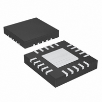
MAX3992UTG+ Maxim Integrated Products, MAX3992UTG+ Datasheet - Page 8

MAX3992UTG+
Manufacturer Part Number
MAX3992UTG+
Description
IC DATA RECOVERY W/EQ 24-TQFN
Manufacturer
Maxim Integrated Products
Type
Clock and Data Recovery (CDR)r
Datasheet
1.MAX3992UTG.pdf
(12 pages)
Specifications of MAX3992UTG+
Input
CML
Output
CML
Frequency - Max
693MHz
Voltage - Supply
3 V ~ 3.6 V
Operating Temperature
0°C ~ 85°C
Mounting Type
Surface Mount
Package / Case
24-TQFN Exposed Pad
Frequency-max
693MHz
Lead Free Status / RoHS Status
Lead free / RoHS Compliant
The MAX3992 clock and data recovery with equalizer
recovers data from the XFI interface. It consists of an
equalizer with LOS power detector and a data retimer
with LOL indicator. An optional recovered clock may
also be enabled for performance testing.
The SDI inputs of the MAX3992 accept serial NRZ data
from XFI standard interfaces. When signals from
400mV
line from 0 to 12 inches of FR-4, the equalizer restores
them for recovery by the CDR. The equalizer removes
10Gbps Clock and Data Recovery
with Equalizer
Figure 3. Functional Diagram
8
_______________________________________________________________________________________
PIN
EP
22
23
24
P-P
REFCLK+
REFCLK-
to 1000mV
SDI+
SDI-
REFCLK-
Exposed
NAME
FCTL1
200Ω
VTH
Pad
CML
P-P
Detailed Description
are applied to a transmission
Negative Reference Clock Input, Digital. The REFCLK inputs are designed to be AC-coupled to the
reference clock source. REFCLK± have a 200Ω differential impedance. See the Detailed Description
section for more information. See Table 2.
Function Control Input 1, TTL. See Table 3 for more information.
LOS Threshold Input, Analog. A voltage applied to this input sets the LOS assert threshold. The LOS
power detector can be disabled if VTH is connected to V
Supply Ground. The exposed pad must be soldered to the circuit-board ground for proper thermal
and electrical performance. The MAX3992 uses exposed-pad variation T2444-4 in the package
outline drawing. See the exposed-pad package.
VTH
EQUALIZER
DETECTOR
LOL
LOL
LOS
Equalizer
FREQUENCY
DETECTOR
PHASE/
MAX3992
most of the deterministic jitter caused by frequency
dependent skin effect and dielectric losses, as well as
connector loss.
The integrated PLL recovers a synchronous clock that
is used to retime the input data. Connect a 0.047µF
capacitor between CFIL and V
ening. The external reference connected to REFCLK
aids in frequency acquisition. Because the reference
clock is only used for frequency acquisition, an
extremely low jitter generation can be achieved from a
low-quality reference clock. The reference clock should
be within ±100ppm of the bit rate divided by 16 or 64.
CFIL
PLL
FUNCTION
Pin Description (continued)
VCO
CC
D
, which forces LOS low.
DFF
FCTL1
FUNCTIONAL
CONTROL
Functional Diagram
Q
POL
FCTL2
CC
CML
CML
to provide PLL damp-
PLL Retimer
SDO+
SDO-
SCLKO+
SCLKO-


