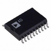
AD800-52BRZ Analog Devices Inc, AD800-52BRZ Datasheet - Page 3

AD800-52BRZ
Manufacturer Part Number
AD800-52BRZ
Description
IC CLK\DATA RECOVERY PLL 20SOIC
Manufacturer
Analog Devices Inc
Type
Clock and Data Recovery (CDR)r
Datasheet
1.AD800-52BRZRL.pdf
(12 pages)
Specifications of AD800-52BRZ
Output
Differential
Frequency - Max
51.84MHz
Operating Temperature
-40°C ~ 85°C
Mounting Type
Surface Mount
Package / Case
20-SOIC (7.5mm Width)
Frequency-max
51.84MHz
Lead Free Status / RoHS Status
Lead free / RoHS Compliant
Voltage - Supply
-
Input
-
Available stocks
Company
Part Number
Manufacturer
Quantity
Price
Part Number:
AD800-52BRZ
Manufacturer:
ADI/亚德诺
Quantity:
20 000
Device
AD800-45BQ
AD800-52BR
AD802-155BR
AD802-155KR
REV. B
ABSOLUTE MAXIMUM RATINGS*
Supply Voltage . . . . . . . . . . . . . . . . . . . . . . . . . . . . . . . . . –6 V
Input Voltage (Pin 16 or Pin 17 to V
Maximum Junction Temperature
Storage Temperature Range . . . . . . . . . . . . –65 C to +150 C
Lead Temperature Range (Soldering 60 sec) . . . . . . . +300 C
ESD Rating
Number Mnemonic
1
2
3
4
5
6
7
8
9
10
11
12
13
14
15
16
17
18
19
20
*Stresses above those listed under “Absolute Maximum Ratings” may cause
permanent damage to the device. This is a stress rating only; functional operation
of the device at these or any other conditions above those indicated in the
operational section of this specification is not implied. Exposure to an absolute
maximum rating condition for an extended period may adversely affect device
reliability.
DATAOUT 50%
SOIC Package . . . . . . . . . . . . . . . . . . . . . . . . . . . . .+150 C
Ceramic DIP Package . . . . . . . . . . . . . . . . . . . . . . +175 C
AD800 . . . . . . . . . . . . . . . . . . . . . . . . . . . . . . . . . . . 1500 V
AD802 . . . . . . . . . . . . . . . . . . . . . . . . . . . . . . . . . . . 1000 V
CLKOUT 50%
(PIN 2)
(PIN 5)
Figure 1. Recovered Clock Skew and Setup
(See Previous Page)
DATAOUT
DATAOUT
V
CLKOUT
CLKOUT
V
V
V
AV
ASUBST
CF
CF
AV
V
V
DATAIN
DATAIN
SUBST
FRAC
FRAC
CC2
EE
EE
CC1
CC1
EE
EE
2
1
CC
Center Frequency
44.736 MHz
51.84 MHz
155.52 MHz
155.52 MHz
PIN DESCRIPTIONS
SETUP TIME
Differential Retimed Data Output
Differential Data Input
Description
Differential Retimed Data Output
Digital Ground
Differential Recovered Clock Output
Differential Recovered Clock Output
Digital V
Digital V
Digital Ground
Analog V
Analog Substrate
Loop Damping Capacitor Input
Loop Damping Capacitor Input
Analog Ground
Digital Ground
Digital V
Differential Data Input
Digital Substrate
Differential Frequency Acquisition
Indicator Output
Differential Frequency Acquisition
Indicator Output
t
SU
EE
EE
EE
RECOVERED CLOCK
EE
CC
) . . . . V
SKEW,
Fractional Loop
Bandwidth
0.1%
0.1%
0.08%
0.08%
t
RCS
EE
to +300 mV
ORDERING GUIDE
Description
20-Pin Cerdip
20-Pin Plastic SOIC
20-Pin Plastic SOIC
20-Pin Plastic SOIC
–3–
GLOSSARY
Maximum and Minimum Specifications
Maximum and minimum specifications result from statistical
analyses of measurements on multiple devices and multiple test
systems. Typical specifications indicate mean measurements.
Maximum and minimum specifications are calculated by adding
or subtracting an appropriate guardband from the typical
specification. Device-to-device performance variation and test
system-to-test system variation contribute to each guardband.
Nominal Center Frequency
This is the frequency that the VCO will operate at with no input
signal present and the loop damping capacitor, C
Tracking Range
This is the range of input data rates over which the PLL will
remain in lock.
Capture Range
This is the range of input data rates over which the PLL can
acquire lock.
Static Phase Error
This is the steady-state phase difference, in degrees, between the
recovered clock sampling edge and the optimum sampling
instant, which is assumed to be halfway between the rising and
falling edges of a data bit. Gate delays between the signals that
define static phase error, and IC input and output signals
prohibit direct measurement of static phase error.
Data Transition Density,
This is a measure of the number of data transitions, from “0” to
“1” and from “1” to “0,” over many clock periods. is the ratio
(0
Jitter
This is the dynamic displacement of digital signal edges from
their long term average positions, measured in degrees rms, or
Unit Intervals (UI). Jitter on the input data can cause dynamic
phase errors on the recovered clock sampling edge. Jitter on the
recovered clock causes jitter on the retimed data.
Output Jitter
This is the jitter on the retimed data, in degrees rms, due to a
specific pattern or some psuedo-random input data sequence
(PRN Sequence).
Jitter Tolerance
Jitter tolerance is a measure of the PLL’s ability to track a jittery
input data signal. Jitter on the input data is best thought of as
phase modulation, and is usually specified in unit intervals.
1) of data transitions to clock periods.
SOIC Package
Cerdip Package
Use of a heatsink may be required depending on operating
environment.
THERMAL CHARACTERISTICS
Operating Temperature
–40 C to +85 C
–40 C to +85 C
–40 C to +85 C
0 C to +70 C
22 C/W
25 C/W
JC
AD800/AD802
75 C/W
90 C/W
Package Option
Q-20
R-20
R-20
R-20
JA
D
, shorted.


