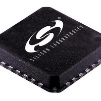
SI5013-BM Silicon Laboratories Inc, SI5013-BM Datasheet - Page 19

SI5013-BM
Manufacturer Part Number
SI5013-BM
Description
IC CLOCK/DATA RECOVERY 28MLP
Manufacturer
Silicon Laboratories Inc
Type
Clock and Data Recovery (CDR)r
Specifications of SI5013-BM
Input
Differential
Output
CML
Frequency - Max
675MHz
Voltage - Supply
3.135 V ~ 3.465 V
Operating Temperature
-40°C ~ 85°C
Mounting Type
Surface Mount
Package / Case
28-VQFN Exposed Pad, 28-HVQFN, 28-SQFN, 28-DHVQFN
Frequency-max
675MHz
Lead Free Status / RoHS Status
Contains lead / RoHS non-compliant
Other names
336-1122
Available stocks
Company
Part Number
Manufacturer
Quantity
Price
Company:
Part Number:
SI5013-BM
Manufacturer:
SILICON
Quantity:
5 000
Part Number:
SI5013-BM
Manufacturer:
SILICONLABS/芯科
Quantity:
20 000
Pin Descriptions: Si5013
Pin #
1
3
4
5
6
SLICE_LVL
Pin Name
REFCLK+
RATESEL
REFCLK–
LOS_LVL
Figure 15. Si5013 Pin Configuration
I/O
Table 8. Si5013 Pin Descriptions
I
I
I
I
SLICE_LVL
RATESEL
REFCLK+
REFCLK–
LOS_LVL
GND
LOL
Signal Level
See Table 2
1
2
3
4
5
6
7
28 27 26 25 24 23 22
8
LVTTL
9
Rev. 1.3
10 11 12 13 14
GND
Pad
Data Rate Select.
This pin configures the onboard PLL for clock and
data recovery at one of two user selectable data
rates. See Table 7 for configuration settings.
Note: This input has a weak internal pullup.
LOS Level Control.
The LOS threshold is set by the input voltage level
applied to this pin. Figure 6 on page 14 shows the
input setting to output threshold mapping.
LOS is disabled when the voltage applied is less
than 1 V.
Slicing Level Control.
The slicing threshold level is set by applying a volt-
age to this pin as described in the Slicing Level sec-
tion of the data sheet. If this pin is tied to GND,
slicing level adjustment is disabled, and the slicing
level is set to the midpoint of the differential input
signal on DIN. Slicing level becomes active when
the voltage applied to the pin is greater than
500 mV.
Differential Reference Clock (Optional).
When present, the reference clock sets the center
operating frequency of the DSPLL for clock and
data recovery. Tie REFCLK+ to VDD and REFCLK–
to GND to operate without an external reference
clock.
See Table 7 on page 13 for typical reference clock
frequencies.
21
20
19
18
17
16
15 TDI
VDD
REXT
RESET/CAL
VDD
DOUT+
DOUT–
Description
Si5013
19


