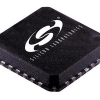
SI5013-BM Silicon Laboratories Inc, SI5013-BM Datasheet - Page 20

SI5013-BM
Manufacturer Part Number
SI5013-BM
Description
IC CLOCK/DATA RECOVERY 28MLP
Manufacturer
Silicon Laboratories Inc
Type
Clock and Data Recovery (CDR)r
Specifications of SI5013-BM
Input
Differential
Output
CML
Frequency - Max
675MHz
Voltage - Supply
3.135 V ~ 3.465 V
Operating Temperature
-40°C ~ 85°C
Mounting Type
Surface Mount
Package / Case
28-VQFN Exposed Pad, 28-HVQFN, 28-SQFN, 28-DHVQFN
Frequency-max
675MHz
Lead Free Status / RoHS Status
Contains lead / RoHS non-compliant
Other names
336-1122
Available stocks
Company
Part Number
Manufacturer
Quantity
Price
Company:
Part Number:
SI5013-BM
Manufacturer:
SILICON
Quantity:
5 000
Part Number:
SI5013-BM
Manufacturer:
SILICONLABS/芯科
Quantity:
20 000
Si5013
20
11,14,18,21,
Pin #
10
25
12
13
15
16
17
19
7
8
9
RESET/CAL
Pin Name
DSQLCH
DOUT+
DOUT–
DIN+
DIN–
GND
VDD
LOS
LOL
LTR
Table 8. Si5013 Pin Descriptions (Continued)
I/O
O
O
O
I
I
I
Signal Level
See Table 2
LVTTL
LVTTL
LVTTL
LVTTL
LVTTL
3.3 V
GND
CML
Rev. 1.3
Loss-of-Lock.
This output is driven low when the recovered clock
frequency deviates from the reference clock by the
amount specified in Table 4 on page 10. If no exter-
nal reference is supplied, this signal will be active
when the internal PLL is no longer locked to the
incoming data.
Lock-to-Reference.
When this pin is low, the DSPLL disregards the data
inputs. If an external reference is supplied, the out-
put clock locks to the supplied reference. If no
external reference is used, the DSPLL locks the
control loop until LTR is released.
Note: This input has a weak internal pullup.
Loss-of-Signal.
This output pin is driven low when the input signal is
below the threshold set via LOS_LVL. (LOS opera-
tion is guaranteed only when ac coupling is used on
the DIN inputs.)
Data Squelch.
When driven high, this pin forces the data present
on DOUT+ to zero and DOUT– to one. For normal
operation, this pin should be low. DSQLCH may be
used during LOS/LOL conditions to prevent random
data from being presented to the system.
Note: This input has a weak internal pulldown.
Supply Voltage.
Nominally 3.3 V.
Differential Data Input.
Clock and data are recovered from the differential
signal present on these pins. AC coupling is recom-
mended.
Production Test Input.
This pin is used during production testing and must
be tied to GND for normal operation.
Differential Data Output.
The data output signal is a retimed version of the
data recovered from the signal present on DIN. It is
phase aligned with CLKOUT and is updated on the
rising edge of CLKOUT.
Reset/Calibrate.
Driving this input high for at least 1 µs will reset
internal device circuitry. A high to low transition on
this pin will force a DSPLL calibration. For normal
operation, drive this pin low.
Note: This input has a weak internal pulldown.
Description


