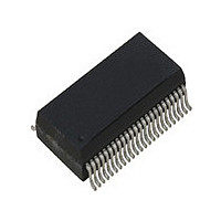
PI6C180BVE Pericom Semiconductor, PI6C180BVE Datasheet - Page 2

PI6C180BVE
Manufacturer Part Number
PI6C180BVE
Description
IC 1:18 CLOCK BUFFER 48-SSOP
Manufacturer
Pericom Semiconductor
Type
Fanout Buffer (Distribution)r
Datasheet
1.PI6C180BVE.pdf
(7 pages)
Specifications of PI6C180BVE
Number Of Circuits
1
Ratio - Input:output
1:18
Differential - Input:output
No/No
Input
TTL
Output
TTL
Frequency - Max
140MHz
Voltage - Supply
3.135 V ~ 3.465 V
Operating Temperature
0°C ~ 70°C
Mounting Type
Surface Mount
Package / Case
48-SSOP
Frequency-max
140MHz
Number Of Outputs
18
Operating Supply Voltage (max)
3.465V
Operating Temp Range
0C to 70C
Propagation Delay Time
8ns
Operating Supply Voltage (min)
3.135V
Mounting
Surface Mount
Pin Count
48
Operating Supply Voltage (typ)
3.3V
Package Type
SSOP
Duty Cycle
55%
Operating Temperature Classification
Commercial
Lead Free Status / RoHS Status
Lead free / RoHS Compliant
Pin Description
OE Functionality
Notes:
1.
2.
I
4, 5, 8, 9
13, 14, 17, 18
31, 32, 35, 36
40, 41, 44, 45
21, 28
11
38
24
25
3, 7, 12, 16,
20, 29, 33, 37,
42, 46
6, 10, 15, 19,
22, 27, 30, 34,
39, 43
23
26
1, 2, 47, 48
2
C Address Assignment
A6
1
Used for test purposes only
Buffers are non-inverting
Pin
06-0109
OE
0
1
A5
1
SDRAM[0-3]
SDRAM[4-7]
SDRAM[8-11]
SDRAM[12-15]
SDRAM[16-17]
Buf_IN
OE
S
S
V
V
V
V
NC
A4
DATA
CLOCK
0
DD[0-9]
SS[0-9]
DDIIC
SSIIC
Symbol
SDRAM[0-17]
A3
1
BUF_IN
Hi-Z
A2
0
O
O
O
O
O
I
I
I/O
I/O
Power
Ground
Power
Ground
Reserved
Type
A1
0
Qty
10
10
A0
4
4
4
4
4
1
1
1
1
1
4
Notes
1
1
2
SDRAM Byte 0 clock output
SDRAM Byte 1 clock output
SDRAM Byte 2 clock output
SDRAM Byte 3 clock output
SDRAM clock outputs usable for feedback
Input for 1-18 buffer
Hi-Z all outputs when held LOW. Has a >100kΩ internal pull-up resistor
Data pin for I
Clock pin for I
3.3V power supply for SDRAM buffers
Ground for SDRAM buffers
3.3V power supply for I
Ground for I
Reserved for future modifications. No connects
R/W
0
2
Serial Configuration Map
Byte0: SDRAM Active/Inactive Register
(1 = enable, 0 = disable)
Note:
1.
2
Bit
2
C circuitry
7
6
5
4
3
2
1
0
C circuitry. Has a >100kΩ internal pull-up resistor
2
Inactive means outputs are held LOW and are disabled from
switching.
C circuitry. Has a >100kΩ internal pull-ip resistor
Pin
18
17
14
13
9
8
5
4
2
C circuitry
SDRAM7 (Active/Inactive)
SDRAM6 (Active/Inactive)
SDRAM5 (Active/Inactive)
SDRAM4 (Active/Inactive)
SDRAM3 (Active/Inactive)
SDRAM2 (Active/Inactive)
SDRAM1 (Active/Inactive)
SDRAM0 (Active/Inactive)
Description
Precision 1-18 Clock Buffer
Description
PS8468B
PI6C180B
06/20/06


