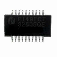
PI49FCT32805QEX Pericom Semiconductor, PI49FCT32805QEX Datasheet - Page 3

PI49FCT32805QEX
Manufacturer Part Number
PI49FCT32805QEX
Description
IC 2X1:5 CLOCK DRIVER 20-QSOP
Manufacturer
Pericom Semiconductor
Series
49FCTr
Type
Fanout Buffer (Distribution)r
Datasheet
1.PI49FCT32805QE.pdf
(7 pages)
Specifications of PI49FCT32805QEX
Number Of Circuits
2
Ratio - Input:output
1:5
Differential - Input:output
No/No
Input
CMOS
Output
CMOS
Frequency - Max
133MHz
Voltage - Supply
2.97 V ~ 3.63 V
Operating Temperature
-40°C ~ 85°C
Mounting Type
Surface Mount
Package / Case
20-QSOP
Frequency-max
133MHz
Number Of Outputs
10
Operating Supply Voltage (max)
3.63V
Operating Temp Range
-40C to 85C
Propagation Delay Time
5.2ns
Operating Supply Voltage (min)
2.97V
Mounting
Surface Mount
Pin Count
20
Operating Supply Voltage (typ)
3.3V
Package Type
QSOP
Quiescent Current
30uA
Power Dissipation
500mW
Input Frequency
133MHz
Operating Temperature Classification
Industrial
Lead Free Status / RoHS Status
Lead free / RoHS Compliant
Available stocks
Company
Part Number
Manufacturer
Quantity
Price
Part Number:
PI49FCT32805QEX
Manufacturer:
PERICOM
Quantity:
20 000
Power Supply Characteristics
Notes:
1.
2.
3.
4.
Parameters
For Max or Min conditions, use appropriate value specified under Electrical Characteristics for the applicable device.
Per TTL driven input (V
This parameter is not directly testable, but is derived for use in Total Power Supply Calculations.
Values for these conditions are examples of the I
ΔI
I
I
CCD
I
CC
C
CC
Description
Quiescent Power
Supply Current
Supply Current per
Inputs @ TTL HIGH
Supply Current per
Output per MHz
IN
= V
CC
(3)
– 0.6V); all other inputs at V
Test Conditions
V
V
V
Outputs Open
OE
50% Duty Cycle
V
Outputs Open
f
50% Duty Cycle
OE
Mon. Outputs Toggling
V
Outputs Open
f
50% Duty Cycle
OE
Eleven Outputs Toggling
O
O
CC
CC
CC
CC
CC
= 10 MH
= 2.5 MH
A
A
A
= Max
= Max
= Max,
= Max,
= Max,
or OE
or OE
or OE
C
formula. These limits are guaranteed but not tested.
B
B
B
Z
Z
= GND
= GND
= GND
(1)
CC
or GND.
3
Condition
V
V
– 0.6V
V
V
V
V
V
V
V
V
V
V
or V
IN
IN
IN
IN
IN
IN
IN
IN
IN
IN
IN
IN
= GND
= V
= V
= GND
= V
= GND
= V
= GND
= V
= GND
= V
= GND
CC
(2)
CC
CC
CC
CC
CC
CC
– 0.6V
– 0.6V
3.3V, 2 x 1:5 CMOS Clock Driver
Min.
Per Output
Toggling
0.09
Typ
110
0.1
1.3
1.3
4.4
4.4
PI49FCT32805
10.0
Max.
9.0
6.0
7.0
0.16
300
30
PS8494C
(4)
(4)
(4)
(4)
Units
MH
mA/
mA
µA
12/19/05
Z


