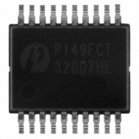
PI49FCT32807HEX Pericom Semiconductor, PI49FCT32807HEX Datasheet - Page 2

PI49FCT32807HEX
Manufacturer Part Number
PI49FCT32807HEX
Description
IC 1:10 CLOCK DRIVER 20-SSOP
Manufacturer
Pericom Semiconductor
Series
49FCTr
Type
Fanout Buffer (Distribution)r
Datasheet
1.PI49FCT32807HE.pdf
(7 pages)
Specifications of PI49FCT32807HEX
Number Of Circuits
1
Ratio - Input:output
1:10
Differential - Input:output
No/No
Input
CMOS
Output
CMOS
Frequency - Max
133MHz
Voltage - Supply
2.97 V ~ 3.63 V
Operating Temperature
-40°C ~ 85°C
Mounting Type
Surface Mount
Package / Case
20-SSOP
Frequency-max
133MHz
Lead Free Status / RoHS Status
Lead free / RoHS Compliant
Available stocks
Company
Part Number
Manufacturer
Quantity
Price
Maximum Ratings
(Above which the useful life may be impaired. For user guidelines, not tested.)
DC Electrical Characteristics
Notes:
1.
2.
3.
4.
5.
Storage Temperature ............................................................ –65°C to +150°C
Ambient Temperature with Power Applied ........................... –40°C to +85°C
Supply Voltage to Ground Potential (Inputs & V
Supply Voltage to Ground Potential (Outputs & D/O Only) .. –0.5V to +7.0V
DC Input Voltage .................................................................... –0.5V to +7.0V
DC Output Current ............................................................................... 120mA
Power Dissipation ................................................................................... 0.5W
V
V
V
V
I
I
V
I
I
I
V
R
Symbol
IH
IL
OH
OL
OS
S
OH
OL
IH
IL
IK
H
For Max. or Min. conditions, use appropriate value specifi ed under Electrical Characteristics for the applicable device type.
Typical values are at V
V
This parameter is determined by device characterization but is not production tested.
Not more than one output should be shorted at one time. Duration of the test should not exceed one second.
OH
08-0298
= V
Output High Voltage
Output Low Voltage
Input High Voltage
Input Low Voltage
Input High Current
Input Low Current
Clamp Diode Voltage
Output HIGH Current
Output LOW Current
Short Circuit
Input Hysteresis
Internal Series Resistor
CC
– 0.6V at rated current.
Parameter
CC
(5)
= 3.3V, +25°C ambient and maximum loading.
Current
(Over the Operating Range)
V
V
Guaranteed Logic HIGH Level (Input pins)
Guaranteed Logic LOW Level (Input pins)
V
V
V
V
V
V
CC
CC
CC
CC
CC
CC
CC
CC
= 3V, V
= 3V V
= 3.6V
= 3.6V
= Min., I
= 3.3V, V
= 3.3V, V
= Max., V
CC
Only) ..... –0.5V to +7.0V
IH
IN
IN
Test Condition
IN
IN
or V
= V
OUT
= -18mA
=V
=V
IH
IL
= GND
IL
IL
or V
2
or V
or V
IL
(5)
IH,
IH,
(1)
V
V
OUT
OUT
I
I
V
V
OH
OL
IN
IN
Note:
Stresses greater than those listed under MAXIMUM
RATINGS may cause permanent damage to the
device. This is a stress rating only and functional op er a tion
of the device at these or any other con di tions above those
indicated in the operational sec tions of this spec i fi ca tion is
not implied. Ex po sure to ab so lute maximum rating condi-
tions for extended pe ri ods may affect re li abil i ty.
= 12mA
= 1.5V
= 1.5V
= -8mA
= 3.6V
= 0V
(5)
(5)
3.3V 1:10 CMOS Clock Driver
Min.
-0.5
-25
-50
2.4
2.0
25
Typ.
-100
-0.7
150
3.0
0.4
-45
45
22
PI49FCT32807
Max.
-180
-1.2
505
-80
0.5
0.8
PS8496B
90
-1
1
Units
mV
mA
μA
11/13/08
Ω
V
V


