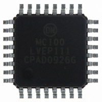
MC100LVEP111FAG ON Semiconductor, MC100LVEP111FAG Datasheet - Page 7

MC100LVEP111FAG
Manufacturer Part Number
MC100LVEP111FAG
Description
IC CLOCK DRIVER DIFF 1:10 32LQFP
Manufacturer
ON Semiconductor
Series
100LVEPr
Type
Fanout Buffer (Distribution), Multiplexerr
Datasheet
1.MC100LVEP111FARG.pdf
(13 pages)
Specifications of MC100LVEP111FAG
Number Of Circuits
1
Ratio - Input:output
2:10
Differential - Input:output
Yes/Yes
Input
ECL, HSTL, LVDS, PECL
Output
ECL, PECL
Frequency - Max
3GHz
Voltage - Supply
2.375 V ~ 3.8 V
Operating Temperature
-40°C ~ 85°C
Mounting Type
Surface Mount
Package / Case
32-LQFP
Frequency-max
3GHz
Output Logic Level
ECL, PECL
Supply Voltage (max)
+/- 3.8 V
Supply Voltage (min)
+/- 2.375 V
Maximum Operating Temperature
+ 85 C
Minimum Operating Temperature
- 40 C
Mounting Style
SMD/SMT
Multiply / Divide Factor
2:1
Number Of Clock Inputs
2
Mode Of Operation
Differential
Output Frequency
3000MHz
Operating Supply Voltage (min)
-2.375/2.375V
Operating Supply Voltage (typ)
-2.5/-3.3/2.5/3.3V
Operating Supply Voltage (max)
-3.8/3.8V
Package Type
LQFP
Operating Temp Range
-40C to 85C
Operating Temperature Classification
Industrial
Signal Type
ECL/HSTL/PECL
Mounting
Surface Mount
Pin Count
32
Lead Free Status / RoHS Status
Lead free / RoHS Compliant
Other names
MC100LVEP111FAGOS
Available stocks
Company
Part Number
Manufacturer
Quantity
Price
Company:
Part Number:
MC100LVEP111FAG
Manufacturer:
ON
Quantity:
3
Company:
Part Number:
MC100LVEP111FAG
Manufacturer:
ON Semiconductor
Quantity:
10 000
NOTE: Device will meet the specifications after thermal equilibrium has been established when mounted in a test socket or printed circuit
14. Measured with 750 mV source, 50% duty cycle clock source. All loading with 50 W to V
15. Skew is measured between outputs under identical transitions and conditions on any one device.
16. Device−to−Device skew for identical transitions at identical V
Table 9. AC CHARACTERISTICS
f
t
t
t
t
V
t
maxPECL/HSTL
PLH
PHL
skew
JITTER
r
/t
PP
f
Symbol
board with maintained transverse airflow greater than 500 lfpm. Electrical parameters are guaranteed only over the declared
operating temperature range. Functional operation of the device exceeding these conditions is not implied. Device specification limit
values are applied individually under normal operating conditions and not valid simultaneously.
Maximum Frequency (Figure 4)
Propagation Delay
(Differential Configuration)
Within−Device Skew (Note 15)
Within−Device Skew @ 2.5 V (Note 15)
Device−to−Device Skew (Note 16)
CLOCK Random Jitter (RMS)
@ v0.5 GHz
@ v1.0 GHz
@ v1.5 GHz
@ v2.0 GHz
@ v2.5 GHz
@ v3.0 GHz
Input Swing (Differential Interconnect
Configuration) Measured Single−Ended
Output Rise/Fall Time (20%−80%)
800
700
600
500
400
300
200
100
Characteristic
0
0
V
CC
1000
= 0 V; V
EE
2000
= −2.375 to −3.8 V or V
Figure 4. F
http://onsemi.com
FREQUENCY (MHz)
Min
325
150
105
CC
3000
levels.
−40°C
0.209
0.200
0.197
0.220
0.232
0.348
7
max
Typ
400
800
200
20
20
85
3
Typical
1200
Max
475
150
255
0.5
0.5
0.4
0.5
0.4
0.6
25
25
4000
CC
= 2.375 to 3.8 V; V
Min
350
150
125
CC
5000
0.204
0.214
0.213
0.224
0.290
0.545
25°C
− 2.0 V.
Typ
430
800
200
20
20
85
3
1200
Max
500
150
275
0.5
0.6
0.5
0.5
0.5
0.8
25
25
6000
EE
= 0 V (Note 14)
Min
375
150
150
0.221
0.229
0.243
0.292
0.522
0.911
85°C
Typ
510
800
230
25
20
85
3
1200
Max
590
150
320
0.5
0.5
0.4
0.6
0.8
1.3
35
25
Unit
GHz
mV
ps
ps
ps
ps


