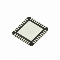
SI5317A-C-GM Silicon Laboratories Inc, SI5317A-C-GM Datasheet - Page 28

SI5317A-C-GM
Manufacturer Part Number
SI5317A-C-GM
Description
IC CLK JITTER CLEANR PROG 36QFN
Manufacturer
Silicon Laboratories Inc
Type
Jitter Cleanerr
Series
Si5317r
Datasheet
1.SI5317C-C-GM.pdf
(46 pages)
Specifications of SI5317A-C-GM
Package / Case
36-QFN
Pll
Yes with Bypass
Input
Clock, Crystal
Output
CML, CMOS, LVDS, LVPECL
Number Of Circuits
1
Ratio - Input:output
1:2
Differential - Input:output
Yes/Yes
Frequency - Max
710MHz
Divider/multiplier
No/No
Voltage - Supply
1.71 V ~ 3.63 V
Operating Temperature
-40°C ~ 85°C
Mounting Type
Surface Mount
Frequency-max
710MHz
Termination Style
SMD/SMT
Output Format
LVPECL
Dimensions
5 mm W x 7 mm L x 1.85 mm H
Minimum Operating Temperature
- 40 C
Maximum Operating Temperature
+ 85 C
Mounting Style
SMD/SMT
Product
XO
Frequency
10 MHz to 945 MHz
Frequency Stability
+/- 20 PPM
Supply Voltage
3.3 Volts
Height
1.85 mm
Lead Free Status / RoHS Status
Lead free / RoHS Compliant
Lead Free Status / RoHS Status
Lead free / RoHS Compliant, Lead free / RoHS Compliant
Other names
336-1923
Si5317
+
SFOUT[1:0] = ML (Output disable)
100
100
CKOUT
Output from
DSPLL
Figure 13. Disable CKOUT Structure
The SFOUT [1:0] pins can also be used to disable both outputs. Disabling the output puts the CKOUT+ and
CKOUT– pins in a high-impedance state relative to V
(common mode tri-state) while the two outputs remain
DD
connected to each other through a 200 on-chip resistance (differential impedance of 200 ). The maximum
amount of internal circuitry is powered down, minimizing power consumption and noise generation (see Figure 13).
Recovery from the disable mode requires additional time as specified in Table 4, “AC Characteristics”.
28
Rev. 1.1


