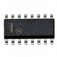
MC14046BDWR2G ON Semiconductor, MC14046BDWR2G Datasheet - Page 6

MC14046BDWR2G
Manufacturer Part Number
MC14046BDWR2G
Description
IC PHASE LOCK LOOP CMOS 16SOIC
Manufacturer
ON Semiconductor
Type
Phase Lock Loop (PLL)r
Datasheet
1.MC14046BCPG.pdf
(8 pages)
Specifications of MC14046BDWR2G
Pll
Yes
Input
CMOS
Output
CMOS
Number Of Circuits
1
Ratio - Input:output
2:2
Differential - Input:output
No/No
Frequency - Max
1.9MHz
Divider/multiplier
No/No
Voltage - Supply
3 V ~ 18 V
Operating Temperature
-55°C ~ 125°C
Mounting Type
Surface Mount
Package / Case
16-SOIC (0.300", 7.5mm Width)
Frequency-max
1.9MHz
Lead Free Status / RoHS Status
Lead free / RoHS Compliant
Other names
MC14046BDWR2GOS
MC14046BDWR2GOS
MC14046BDWR2GOSTR
MC14046BDWR2GOS
MC14046BDWR2GOSTR
Available stocks
Company
Part Number
Manufacturer
Quantity
Price
Company:
Part Number:
MC14046BDWR2G
Manufacturer:
ON Semiconductor
Quantity:
500
Part Number:
MC14046BDWR2G
Manufacturer:
ON/安森美
Quantity:
20 000
NOTE: Sometimes R3 is split into two series resistors each R3
Definitions: N = Total division ratio in feedback loop
PC1
VCO
PCA
PCB
@ FREQUENCY f
out
(a)
INPUT
in
in
in
C
the damping, R4 ^ (0.1)(R3) for optimum results.
PCA
C
should be such that the corner frequency of this network does not significantly affect W
in
K VCO +
K = V
K = V
for a typical design W
PCB
Phase Comparator 1
R3
in
C2
DD
DD
14
/ for Phase Comparator 1
/4
2 p D f VCO
3
V DD – 2 V
Note: for further information, see:
(1) F. Gardner, “Phase−Lock Techniques”, John Wiley and Son, New York, 1966.
(2) G. S. Moschytz, “Miniature RC Filters Using Phase−Locked Loop”, BSTJ, May, 1965.
(3) Garth Nash, “Phase−Lock Loop Design Fundamentals”, AN−535, Motorola Inc.
(4) A. B. Przedpelski, “Phase−Locked Loop Design Articles”, AR254, reprinted by Motorola Inc.
for Phase Comparator 2
2f C [ 1 p
Figure 3. General Phase−Locked Loop Connections and Waveforms
OUTPUT
COMPARATOR
PHASE
n
^
^ 0.707
2 p f r
R3 C2
10
2 p f L
2 OR 13
PC1
PC2
OR
(at phase detector input)
out
out
V
V
V
V
V
V
V
V
DD
SS
OH
OL
OH
OL
OH
OL
(a)
INPUT
Typical Low−Pass Filters
EXTERNAL
LOW-PASS
EXTERNAL
COUNTER
FILTER
http://onsemi.com
N
Waveforms
VCO
2. A capacitor C
R3
in
6
9
R4
C2
R1
11
OUTPUT
w n +
z +
F(s) +
9
R2
C
is then placed from the midpoint to ground. The value for
12
FOLLOWER
2K f K VCO
PC2
SOURCE
Filter A
VCO
PCA
PCB
VCO
Nw n
R 3 C 2 S ) 1
LD
out
K f K VCO
6
in
in
in
NR 3 C 2
CI
A
1
CI
Typically:
R 4 C 2 + 6N
(R 3 ) 3, 000W) C 2 + 100NDf
D f = f
LOW−PASS FILTER
10
7
n
CI
Phase Comparator 2
. In Figure B, the ratio of R3 to R4 sets
B
max
4
w n +
z + 0.5 w n (R 3 C 2 )
F(s) +
− f
f max
R
min
SF
S(R 3 C 2 ) R 4 C 2 ) ) 1
SF
–
NC 2 (R 3 ) R 4 )
out
2 p D f
K f K VCO
@ FREQUENCY Nf = f
Filter B
R 3 C 2 S ) 1
N
f max 2
VCO
K f K VCO
out
– R 4 C 2
N
V
V
V
V
V
V
V
V
V
V
)
DD
SS
OH
OL
OH
OL
OH
OL
OH
OL


