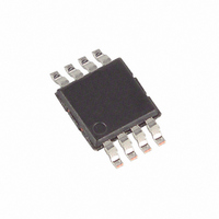
DS1094LU-42M+T Maxim Integrated Products, DS1094LU-42M+T Datasheet - Page 8

DS1094LU-42M+T
Manufacturer Part Number
DS1094LU-42M+T
Description
IC ECONOSCILLATOR SS 8-USOP
Manufacturer
Maxim Integrated Products
Series
EconOscillator™r
Type
Clock Generatorr
Datasheet
1.DS1094LU-42M.pdf
(11 pages)
Specifications of DS1094LU-42M+T
Pll
No
Input
Clock
Output
Clock
Number Of Circuits
1
Ratio - Input:output
2:4
Differential - Input:output
No/No
Frequency - Max
2MHz
Divider/multiplier
Yes/No
Voltage - Supply
3 V ~ 3.6 V
Operating Temperature
-40°C ~ 85°C
Mounting Type
Surface Mount
Package / Case
8-MSOP, Micro8™, 8-uMAX, 8-uSOP,
Frequency-max
2MHz
Lead Free Status / RoHS Status
Lead free / RoHS Compliant
will dither between 2MHz and 1.96MHz at a modulation
frequency determined by the selected dither frequen-
cy. Continuing with the same example, if D1 and D0
both equal zero, selecting f
frequency would be 15.625kHz.
The 2-wire serial interface is used to read and write the
control registers of the DS1094L. The default slave
address of the DS1094L is B0h (see Figure 4). Using
the 3 address bits (A2, A1, and A0) in the ADDR regis-
ter, the slave address can be changed to allow as
many as eight DS1094Ls reside on the same 2-wire
bus or to simply prevent address conflicts with other 2-
wire devices. The location of the address bits within the
ADDR register is shown in the Control Registers sec-
tion. A detailed description of the 2-wire interface is
found in the 2-Wire Serial Interface Description section.
Since EEPROM does have a limited number of lifetime
write cycles (specified in the NONVOLATILE MEMORY
CHARACTERISTICS electrical table), it is possible to
configure the DS1094L to prevent EEPROM wear out
and eliminate the EEPROM write cycle time by using
the WC bit in the ADDR register. When the WC bit is 0
(default), register writes are automatically written into
EEPROM. The Write EE Command is not needed.
However, if WC = 1, then register writes are stored in
SRAM and only written to EEPROM when the user
sends the Write EE Command. If power to the device is
cycled, the last value stored in EEPROM is recalled.
The time required to store the values is one EEPROM
write cycle time. WC = 1 is ideal for applications that
frequently modify the frequency/registers.
Regardless of the value of the WC bit, the value of the
ADDR register is always written immediately to EEP-
ROM.
The DS1094L control registers are used to program the
frequency and features of the device. Table 6 lists the
Multiphase Spread-Spectrum EconOscillator
Table 6. Control Registers
X = Don’t care
X
8
PRESCALER
DAC
ADDR
WRITE EE Command
1
= Don’t care, reads as 1
_____________________________________________________________________
REGISTER
ADDRESS
EEPROM Write Control
0Dh
02h
08h
3Fh
2-Wire Slave Address
MOSC
Control Registers
/128, then the dither
MSB
D1
X
X
1
1
D0
X
X
1
1
Ph1
X
X
1
1
Ph0
X
X
BINARY
No Data
1
1
WC
D3
J1
DS1094L’s control registers and illustrates bit locations
as well as other valuable information. The memory
address of each register is shown in the ADDRESS col-
umn. The factory default values programmed into EEP-
ROM are shown in the DEFAULT column. Refer to the
corresponding sections to determine what values to
write to the registers.
PRESCALER (02h)
D1, D0
Ph1, Ph0 Determines whether the two-phase, three-
J1, J0
P1, P0
DAC (08h)
D3 to D0 This four-bit value determines the master oscil-
ADDR (0Dh)
WC
A2 to A0 This three-bit value determines the 2-wire
WRITE EE COMMAND (3Fh)
This command can be used when the WC bit = 1 (see
explanation in the EEPROM Write Control section) to
transfer registers internally from SRAM to EEPROM. The
time required to store the values is one EEPROM write
cycle time. This command is not needed if WC = 0.
D2
A2
J0
Selects the dither frequency. Refer to Table 5.
Selects the dither amount. Refer to Table 4.
phase, or four-phase mode is selected. Refer
to Table 3.
Determines the prescaler value. Refer to
Table 2.
lator frequency, f
the Master Oscillator section for a detailed
information on calculating the DAC value.
The EEPROM write control bit determines if
writes to control registers are automatically
backed up in NV memory (EEPROM) or
whether a write EE command is required to
write to NV memory. See the EEPROM Write
Control section for more information.
slave address.
D1
A1
P1
LSB
D0
A0
P0
XXXX0000b
XXXX0000b
11001101b
DEFAULT
MOSC
. Refer to Table 1 and
ACCESS
R/W
R/W
R/W
W


